Ge/Sb type superlattice phase-change film material for high-speed low-power phase-change memory and preparation method of material

A technology of phase-change memory and thin-film materials, applied in nanotechnology for materials and surface science, metal material coating technology, ion implantation plating, etc., can solve the problem of not fully meeting the requirements of semiconductor chips and information storage , poor film thermal stability and other issues, to achieve the effects of shortening the crystallization time, inhibiting crystallization, and low power consumption

Active Publication Date: 2015-09-23
JIANGSU UNIV OF TECH
View PDF8 Cites 16 Cited by
  • Summary
  • Abstract
  • Description
  • Claims
  • Application Information

AI Technical Summary

Problems solved by technology

First of all 2 Sb 2 Te 5 The nucleation-based crystallization mechanism of the thin film makes its phase transition slow, which cannot meet the information storage requirements of the future high-speed and big data era; secondly, Ge 2 Sb 2 Te 5 The t

Method used


Image

  • Ge/Sb type superlattice phase-change film material for high-speed low-power phase-change memory and preparation method of material
  • Ge/Sb type superlattice phase-change film material for high-speed low-power phase-change memory and preparation method of material

Examples


Embodiment 1)

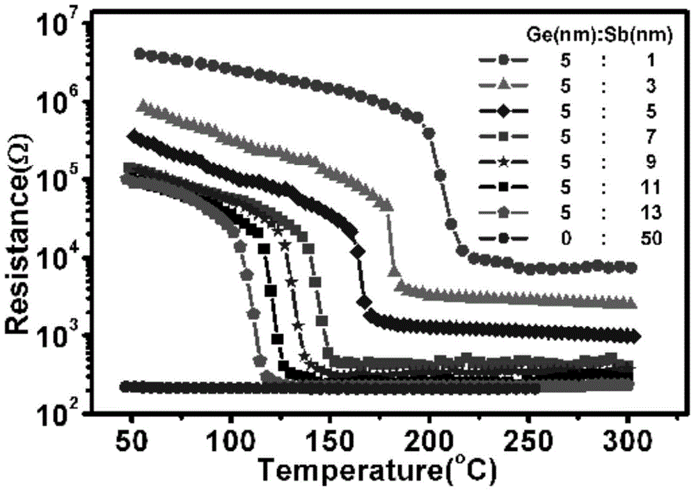
[0027] The Ge / Sb-based superlattice phase-change thin film material used for high-speed and low-power phase-change memory in this embodiment is a multilayer film structure with a thickness of 6-80 nm; it is formed by alternately depositing and compounding Ge layers and Sb layers, namely In the thin film, the sequence of Ge layer-Sb layer-Ge layer-Sb layer... is repeated and alternately arranged. One layer of Ge and one layer of Sb are used as an alternating cycle, and the Ge layer of the latter alternate cycle is deposited on the Sb layer of the previous alternate cycle.

[0028] The general formula [Ge(a) / Sb(b)] for the film structure of the above-mentioned GeSb-based superlattice phase-change thin film material x where a is the thickness of a single layer of Ge, 1nm≤a≤50nm; b is the thickness of a single layer of Sb, 1nm≤b≤50nm; x is the number of alternating cycles of Ge and Sb layers, or a layer of Ge layer and a layer of Sb as a group, and the film material is composed of ...

Embodiment 2)

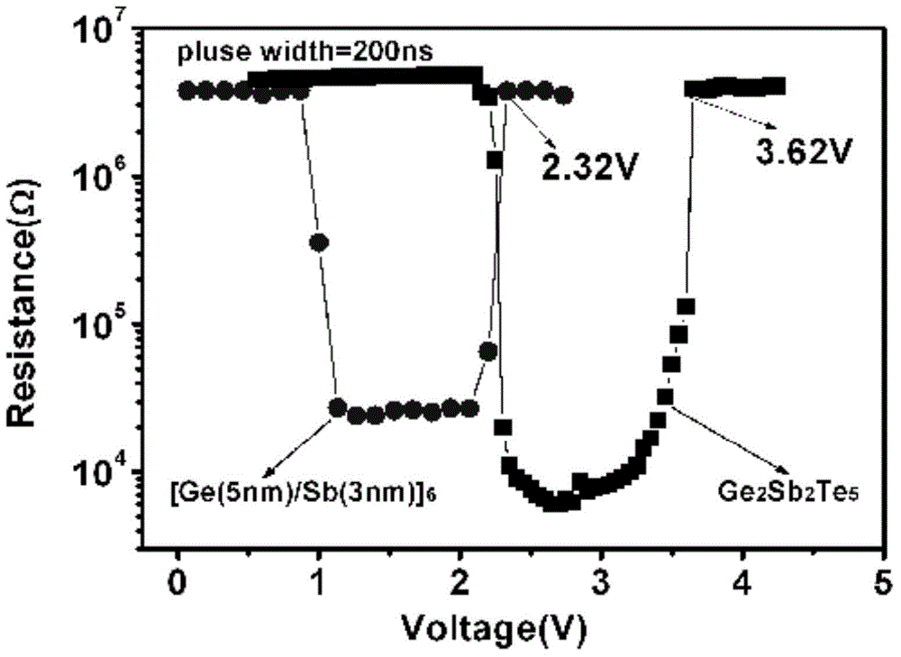
[0042] The film structure of the Ge / Sb class superlattice phase-change film material used for high-speed low-power phase-change memory of the present embodiment is [Ge (5nm) / Sb (3nm)] 6 , that is, the thickness of each layer of Ge layer is 5nm, the thickness of each layer of Sb layer is 3nm, the number of alternating periods of Ge layer and Sb layer is 6, and the thickness of Ge / Sb superlattice phase change thin film material is 48nm.

[0043] All the other preparation methods are the same as in Example 1, the difference is: step 3. magnetron sputtering preparation [Ge(a) / Sb(b)] x For multilayer composite films, the sputtering time of each layer of Sb is 9s. The Ge layer and the Sb layer were alternately sputtered 6 times.

Embodiment 3)

[0045] The film structure of the Ge / Sb class superlattice phase-change film material used for high-speed low-power phase-change memory of the present embodiment is [Ge (5nm) / Sb (5nm)] 6 , that is, the thickness of each layer of Ge layer is 5nm, the thickness of each layer of Sb layer is 5nm, the number of alternating cycles of Ge layer and Sb layer is 6, and the thickness of Ge / Sb superlattice phase change thin film material is 60nm.

[0046] All the other preparation methods are the same as in Example 1, the difference is: step 3. magnetron sputtering preparation [Ge(a) / Sb(b)] x For multilayer composite films, the sputtering time for each layer of Sb is 15s. Ge layer and Sb layer were alternately sputtered 6 times.


PUM

PropertyMeasurementUnit
Thicknessaaaaaaaaaa
Thicknessaaaaaaaaaa
Thicknessaaaaaaaaaa

Abstract

The invention discloses a Ge/Sb type superlattice phase-change film material for a high-speed low-power phase-change memory. The material is characterized in that the material of a multilayer film structure is formed by depositing and combining Ge and Sb layers alternatively, one Ge layer and one Sb layer serve as an alternative period, and the Ge layer of the latter alternative layer is deposited on the Sb layer of the former alternative period. The Ge/Sb type superlattice phase-change film material utilizes the clamping effect of a multilayer interface in the superlattice structure, the size of the crystal grains is reduced, the crystallization time is shortened, crystallization is inhibited, the thermal stability of the material is improved, and the phase change speed is improved. The RESEST voltage of the Ge/Sb type superlattice phase-change film material is over 30% lower than that of a GE2Sb2Te5 film under the same voltage pulses, and thus, the power consumption of the Ge/Sb type superlattice phase-change film material is lower.

Description

technical field [0001] The invention relates to a phase change thin film material in the technical field of microelectronics, in particular to a Ge / Sb superlattice phase change thin film material used for a high-speed, low power consumption phase change memory and a preparation method thereof. Background technique [0002] Phase Change Random Access Memory (Phase Change Random Access Memory, abbreviated as PCRAM) has a long cycle life (>10 13 Times), small component size, high storage density, fast reading speed, strong stability, high and low temperature resistance (-55 ° C ~ 125 ° C), anti-vibration, and compatibility with existing integrated circuit technology, etc., so it is more and more popular More and more researchers and enterprises are paying attention (Kun Ren et al., Applied Physics Letter, 2014, 104(17): 173102). PCRAM uses the huge resistance difference between the material in the crystalline state and the amorphous state to store information. When the phas...

Claims


Application Information

Patent Timeline
IPC IPC(8): H01L45/00B82Y30/00B82Y40/00C23C14/35C23C14/16C23C14/18
Inventor 胡益丰朱小芹吴世臣邹华袁丽吴卫华张建豪眭永兴沈大华
Owner JIANGSU UNIV OF TECH
Why Eureka
Try Eureka