Terminal structure of super-junction semiconductor device and manufacturing method thereof

A technology of superjunction semiconductor and terminal structure, applied in semiconductor/solid-state device manufacturing, semiconductor devices, electrical components, etc., can solve the problems of high process standard, difficult realization of manufacturing process, high complexity of terminal structure, low cost, High reliability and small size effect

Inactive Publication Date: 2015-09-30
ADVANCED SEMICON MFG CO LTD
View PDF11 Cites 6 Cited by
  • Summary
  • Abstract
  • Description
  • Claims
  • Application Information

AI Technical Summary

Problems solved by technology

[0008] The technical problem to be solved by the present invention is to overcome the high complexity of the terminal structure of the super-junction semiconductor device in the prior art, so the manufacturing process is difficult to realize and the process standard is high Shortcomings, providing a terminal structure of a super junction semiconductor device and a manufacturing method thereof

Method used


Image

  • Terminal structure of super-junction semiconductor device and manufacturing method thereof
  • Terminal structure of super-junction semiconductor device and manufacturing method thereof
  • Terminal structure of super-junction semiconductor device and manufacturing method thereof

Examples


Embodiment 1

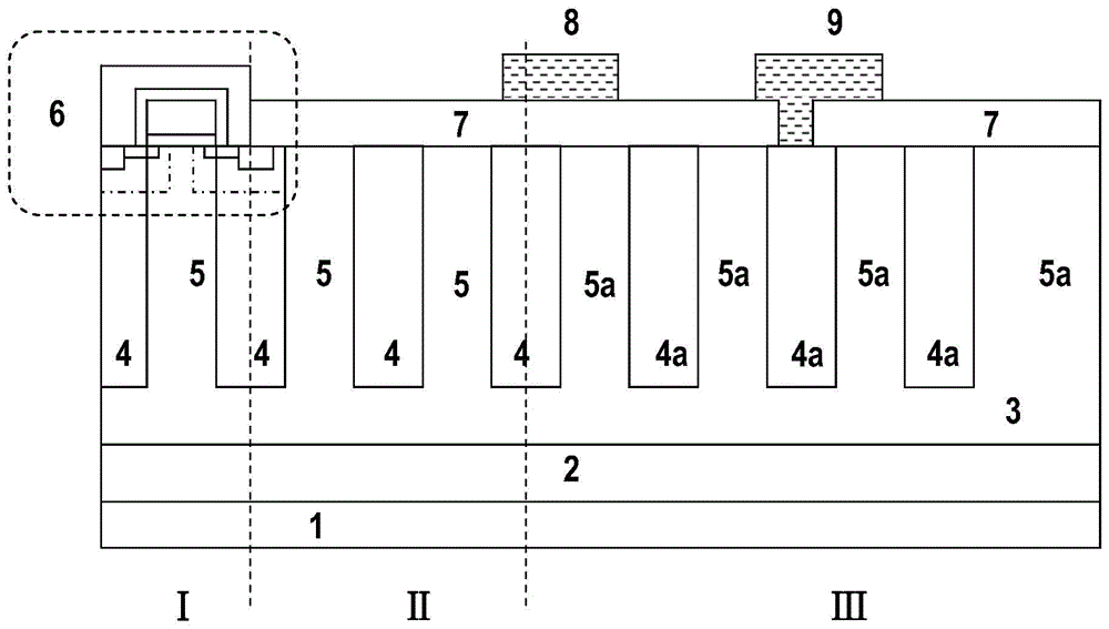
[0066] Such as figure 2 As shown, the terminal structure of the super junction semiconductor device of this embodiment has several super junction P columns, each super junction P column includes a top P column and a bottom P column, and the top P column in each super junction P column The width is not less than the width of the bottom P-pillar.

[0067] Among the several superjunction P columns, the top P columns located in the transition region of the terminal structure are connected to each other, and the spacing between the top P columns located in the terminal region of the terminal structure is along the transition away from the terminal structure The direction of the zone gradually widens.

[0068] Each top P-pillar is 2-6 microns in height. And the top P pillars of the plurality of super junction P pillars are formed by ion implantation and annealing activation.

Embodiment 2

[0070] Combine below Attached picture A method of manufacturing the terminal structure of the super junction semiconductor device of the second embodiment will be described. The manufacturing method of this embodiment is applicable to the epitaxial super junction structure. The flow of the manufacturing method of this embodiment picture Can refer to figure 1 9, the details are as follows.

[0071] Step 1, see image 3 , using an epitaxial process to epitaxially form a 3-15um N-type epitaxial layer 3-1 on the N-type heavily doped silicon substrate 2;

[0072] Step 2. Repeat the following operations several times until a bottom P-pillar with a preset height is obtained: first see Figure 4 As shown, use the designed bottom P-pillar mask to perform photolithography mask PR, P-type ion implantation 4b-1, and then see Figure 5 As shown, after degelling and cleaning, the epitaxy of the N-type epitaxial layer 3-2 is continued.

[0073] When the following operations ...

Embodiment 3

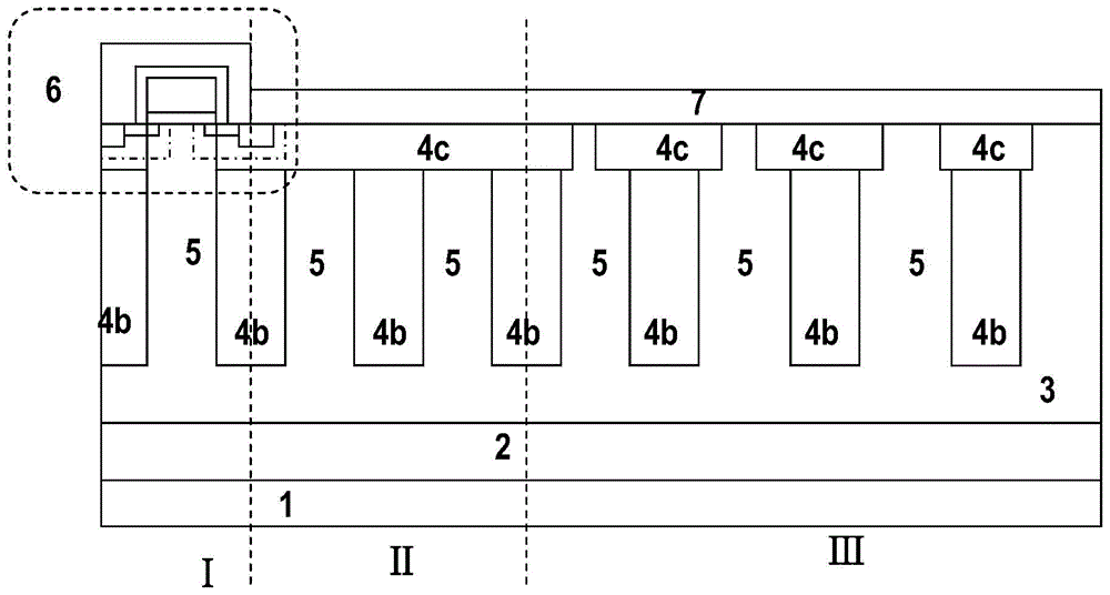
[0089] Combine below Attached picture A method of manufacturing the terminal structure of the super junction semiconductor device of the third embodiment will be described. The manufacturing method of this embodiment is applicable to a trench type super junction structure.

[0090] Step 1, see figure 1 4. Using an epitaxial process, an N-type epitaxial layer 3 of 10-100 microns is epitaxially grown on an N-type heavily doped silicon substrate 2;

[0091] Step two, see figure 1 5. Etching the deep trench 4d-1 required for the P-pillar by means of deep trench etching;

[0092] Step three, see figure 1 6. Fill the material 4d containing P-type impurities, such as P-type single crystal silicon epitaxy, and use chemical mechanical polishing (CMP) to flatten the silicon surface;

[0093] Step 4, see figure 1 6. Use the designed top P-pillar mask and photolithography mask to complete top P-type ion implantation 4c-1 and gel removal;

[0094] Step seven, see Figure 8...


PUM


Abstract

The invention discloses a terminal structure of a super-junction semiconductor device and a manufacturing method thereof. The terminal structure comprises a plurality of super-junction P-pillars; each super-junction P-pillar comprises a top P-pillar and a bottom P-pillar; the top P-pillar of each super-junction P-pillar is narrower than the bottom P-pillar thereof. The thermal structure and the manufacturing method thereof have the advantages that the terminal structure can be high in reliability and small in size, the cost is low, the process is simple and easy to implement and a process window is wide.

Description

technical field [0001] The invention relates to a super junction semiconductor device, in particular to a terminal structure of a super junction semiconductor device and a manufacturing method thereof. Background technique [0002] Since the invention of super junction semiconductor devices in 1991 (see US patent US5216275), after more than 20 years of technical improvement, a 600V-900V super junction metal oxide semiconductor field effect transistor (Super Junction MOSFET) has been successfully developed, which is widely used in power Electronic equipment, such as power switches, motor drives, DC-DC converters and other fields. [0003] The core structure of a superjunction device is a P-type doped semiconductor column (referred to as the P column) and an N-type doped semiconductor column (referred to as the N column) arranged vertically below the surface of the device (hereinafter referred to as the vertical direction) alternately. Charge balance condition. The principle...

Claims


Application Information

Patent Timeline
Patent Type & Authority Applications(China)
IPC IPC(8): H01L29/06H01L29/78H01L21/336
CPCH01L29/0634H01L29/66477H01L29/78
Inventor 高文玉陶有飞徐雷军刘启星
Owner ADVANCED SEMICON MFG CO LTD
Why Eureka
Try Eureka