Backside-illuminated image sensor wafer level packaging process and packaging structure

An image sensor, wafer-level packaging technology, applied in radiation control devices and other directions, can solve the problems of poor physical support, residual glue in the photosensitive area, limited photon absorption capacity, etc.

Active Publication Date: 2015-10-21
NAT CENT FOR ADVANCED PACKAGING
View PDF3 Cites 9 Cited by
  • Summary
  • Abstract
  • Description
  • Claims
  • Application Information

AI Technical Summary

Problems solved by technology

The protective cover is transparent, but when the pixel capacity of the chip reaches more than 5 million, the area of ​​a single pixel becomes smaller, and the ability to absorb photons is limited, so the tiny refraction and reflection of photons by the original protective cover will be reduced. Affects the pixel's ability to sense light. For large pixel image sensors, the protective cover must be removed
[0005] Because the CIS wafer is only about 5um in thickness, the physical support ability is poor. Before the protective cover is supported by a mesh photoresist wall for bonding process, the cover and the wafer are connected by a photoresist wall. Uneven force on the surface can easily cause cracks on the photosensitive surface of the CIS wafer in the subsequent TSV and RDL processes
And if the surface of the protective cover is all glued, then when the cover is removed later, there may be residual glue in the photosensitive area

Method used


Image

  • Backside-illuminated image sensor wafer level packaging process and packaging structure
  • Backside-illuminated image sensor wafer level packaging process and packaging structure
  • Backside-illuminated image sensor wafer level packaging process and packaging structure

Examples


Embodiment 1

[0036] A wafer-level packaging process for a back-illuminated image sensor of the present invention comprises the following steps:

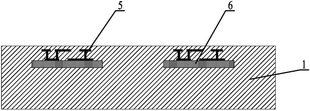
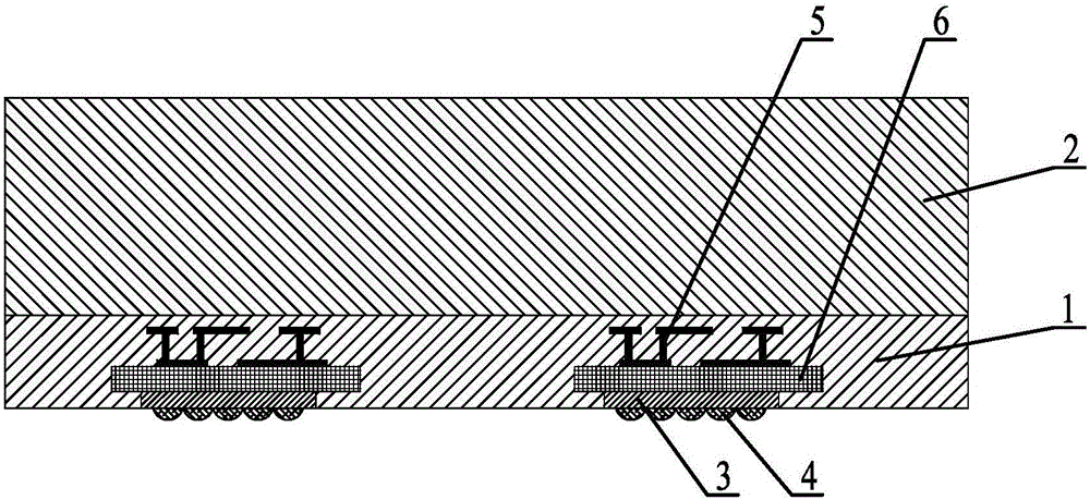
[0037] a. Take the CIS wafer 1 on which the leads 5 and the image sensor 6 have been made on the front side. The thickness of the CIS wafer 1 is 50 μm, and the thickness of the CIS wafer 1 is bonded by a conventional silicon-silicon bonding method A 200um load wafer 2 is supported by the load wafer 2 to thin the back of the CIS wafer 1, and a filter 3 and a microlens 4 are placed on the back of the thinned CIS wafer 1, such as figure 1 shown;

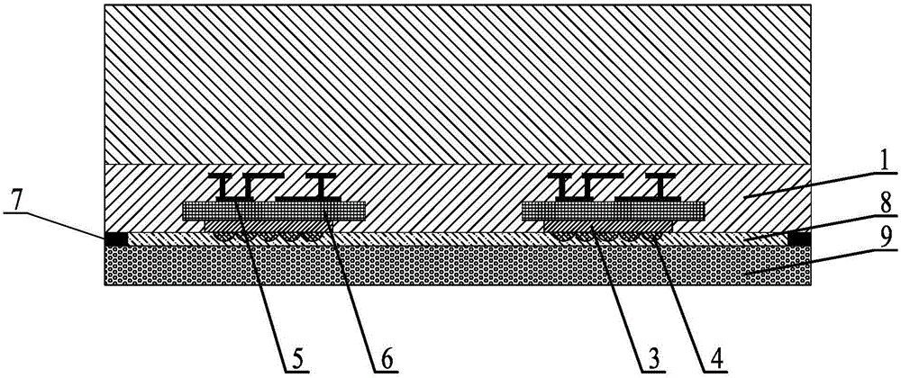
[0038] b. The edge position of the back side of the CIS wafer 1 is covered by the first adhesive glue 7 in a coating method. The material of the first adhesive glue 7 is benzocyclobutene. The backside edge of wafer 1 forms a closed ring, the width of the first bonding glue 7 is 1mm and the thickness of the first bonding glue is 10nm, coats with the second bonding glue 8 in this closed ring, the second Th...

Embodiment 2

[0042] A wafer-level packaging process for a back-illuminated image sensor of the present invention comprises the following steps:

[0043] a. Take the CIS wafer 1 on which the leads 5 and the image sensor 6 have been made on the front side. The thickness of the CIS wafer 1 is 100 μm, and the thickness of the CIS wafer 1 is bonded by conventional silicon-oxygen bonding method A 300um load wafer 2 is supported by the load wafer 2 to thin the back of the CIS wafer 1, and a filter 3 and a microlens 4 are placed on the back of the thinned CIS wafer 1, such as figure 1 shown;

[0044] b. Cover the edge position of the back side of the CIS wafer 1 by spraying the first adhesive glue 7, the material of the first adhesive glue 7 is thermoplastic epoxy resin, and the first adhesive glue 7 is placed on the CIS wafer The back edge of 1 forms a closed ring, the width of the first bonding glue is 2mm and the thickness of the first bonding glue is 1um, and the second bonding glue 8 is used...

Embodiment 3

[0048] A wafer-level packaging process for a back-illuminated image sensor of the present invention comprises the following steps:

[0049] a. Take the CIS wafer 1 on which the leads 5 and the image sensor 6 have been made on the front, the thickness of the CIS wafer 1 is 150 μm, and the thickness of the CIS wafer 1 is bonded by conventional oxygen-oxygen bonding method A 400 um load wafer 2 is supported by the load wafer 2 to thin the back of the CIS wafer 1, and a filter 3 and a microlens 4 are placed on the back of the thinned CIS wafer 1, such as figure 1 shown;

[0050] b. The edge position on the back side of the CIS wafer 1 is covered by the first adhesive glue 7 in a film-pasting manner. The material of the first adhesive glue 7 is UV epoxy resin, and the first adhesive glue 7 is placed on the CIS wafer. The back edge of 1 forms a closed ring, the width of the first adhesive glue is 3mm and the thickness of the first adhesive glue is 100um, and the second adhesive glu...


PUM


Abstract

The invention relates to a backside-illuminated image sensor wafer-level packaging process and packaging structure. The packaging process comprises the following steps: bonding a load wafer on the front surface of a CIS wafer, thinning the back surface of the CIS wafer with the load wafer being as a support, and preparing a light filter and a micro lens on the back surface of the thinned CIS wafer; carrying out covering on the edge position of the back surface of the CIS wafer with first bonding glue, carrying out coating with second bonding glue in an enclosed annular shape, and bonding a seal cover onto the back surfaces of the first bonding glue and the second bonding glue; thinning the load wafer with the seal cover being as a support, preparing conductive columns in the thinned load wafer, and depositing a conductive layer on the top end of each conductive column; and removing stickiness of the first bonding glue to enable the CIS wafer and the seal cover to be separated, cleaning the CIS wafer and the seal cover to remove the second bonding glue, and finally, carrying out cutting to obtain the backside-illuminated image sensor wafer-level packaging structure. The process reduces the thickness of the package wafer and can enable the seal cover to be used repeatedly.

Description

technical field [0001] The invention not only discloses a wafer-level packaging process for a back-illuminated image sensor, but also discloses a wafer-level packaging structure for a back-illuminated image sensor, which belongs to the technical field of semiconductor packaging. Background technique [0002] In recent years, as the pixel value of the image sensor (CIS) chip has become larger and larger, the physical size of a single pixel of the sensor has become smaller and smaller, so that the integrated circuit manufacturing process for the sensor part of the chip has become more and more complicated, so that the Parts have been difficult to manufacture in the same process as the signal processing module. In addition, since the photosensitive area of ​​a single pixel is getting smaller and smaller, in order to prevent image distortion, it also has a strict limit on the amount of incident photons. [0003] In the previous wafer-level packaging, the interconnection line wa...

Claims


Application Information

Patent Timeline
Patent Type & Authority Applications(China)
IPC IPC(8): H01L27/146
Inventor 冯光建靖向萌
Owner NAT CENT FOR ADVANCED PACKAGING
Why Eureka
Try Eureka