
Method for preparing quantum dot photodetection array device based on ink-jet printing technology

An inkjet printing and light detection technology, which is applied in the manufacturing of semiconductor devices, electrical components, and final products, etc., can solve the problems of wasting materials and complicated preparation processes, and achieves strong controllability, simple and convenient process operation, and good recovery. sexual effect

Inactive Publication Date: 2015-10-21
FUZHOU UNIV
View PDF5 Cites 27 Cited by
  • Summary
  • Abstract
  • Description
  • Claims
  • Application Information

AI Technical Summary

Problems solved by technology

According to this characteristic, there are related quantum dot photodetection researches in the prior art, but the preparation process of photodetectors in the current research is complicated and wastes materials, while inkjet printing technology has advantages that other technologies do not have. If you use inkjet, you can just print where you want to print, and there will be no material waste, and because it is in the form of a printing array, you can properly cut the photodetector device according to your needs in the later stage. This can be said that only inkjet Advantages of ink-printed devices

Method used


Image

  • Method for preparing quantum dot photodetection array device based on ink-jet printing technology
  • Method for preparing quantum dot photodetection array device based on ink-jet printing technology
  • Method for preparing quantum dot photodetection array device based on ink-jet printing technology

Examples


Embodiment 1

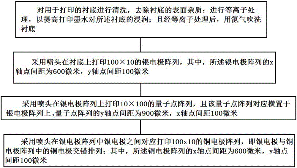
[0045] Step S1: ultrasonically clean the common PET substrate used for printing with acetone, ethanol and deionized water for 15 minutes to remove surface impurities of the common PET substrate; perform plasma treatment for 10 minutes to improve the printing ink’s effect on the common PET substrate. Wetting of the substrate; and after plasma treatment, purging the common PET substrate with nitrogen; in the present embodiment, the common PET substrate is plasma treated and soaked in chloroform to improve The surface roughness of the common PET substrate.

[0046] Step S2: using an inkjet printer jetlab2 to print a 100×10 silver electrode array on the ordinary PET substrate with an 80-micron nozzle, and heat-treat the silver electrodes at a temperature of 80 degrees Celsius after printing, wherein the silver electrode array The x-axis point spacing is 600 microns, the y-axis point spacing is 100 microns, the thickness of the silver electrode is 50 nanometers, and the pri...

Embodiment 2

[0051] Step S1: ultrasonically clean the ordinary PET substrate used for printing with acetone, ethanol and deionized water for 15 minutes to remove surface impurities of the ordinary PET substrate; perform plasma treatment for 10 minutes to improve the printing ink's resistance to the ordinary PET substrate. Wetting of the PET substrate; and after the plasma treatment, the ordinary PET substrate is purged with nitrogen; in this embodiment, the ordinary PET substrate is plasma treated and soaked in chloroform for Improve the surface roughness of the common PET substrate.

[0052] Step S2: using an inkjet printer jetlab2 to print a 100×10 silver electrode array on the ordinary PET substrate with an 80-micron nozzle, and heat-treat the silver electrodes at a temperature of 80 degrees Celsius after printing, wherein the silver electrode array The x-axis point spacing is 600 microns, the y-axis point spacing is 100 microns, the thickness of the silver electrode is 50 na...

Embodiment 3

[0057] Step S1: ultrasonically clean the common glass substrate used for printing with acetone, ethanol and deionized water for 15 min to remove the surface impurities of the common glass substrate; perform plasma treatment for 10 min to improve the printing ink’s resistance to the common glass substrate. Wetting of the glass substrate; and after the plasma treatment, the ordinary glass substrate is purged with nitrogen; in this embodiment, the ordinary glass substrate is subjected to plasma treatment and soaked in chloroform for Improve the surface roughness of the common glass substrate.

[0058] Step S2: using an inkjet printer jetlab2 to print a 100×10 silver electrode array on the ordinary glass substrate with an 80-micron nozzle, and heat-treat the silver electrodes at a temperature of 80 degrees Celsius after printing, wherein the silver electrode array The x-axis point spacing is 600 microns, the y-axis point spacing is 100 microns, the thickness of the silver ...


PUM

PropertyMeasurementUnit
thicknessaaaaaaaaaa
thicknessaaaaaaaaaa
thicknessaaaaaaaaaa

Abstract

The invention relates to a method for preparing a quantum dot photodetection array device based on ink-jet printing technology. The method is characterized by carrying out plasma and chloroform processing on a substrate; then, printing a metal electrode array and a quantum dot array on the substrate through an ink-jet printer with metal electrode ink and quantum dot ink respectively; and finally, carrying out current and voltage test in the dark and any monochromatic light source environment. The method for preparing the quantum dot photodetection array device based on the ink-jet printing technology is simple in preparation technology, and can carry out large-scale production; and the photodetection device adopts quantum dots, so that the photodetection device has a better photosensitive characteristic for any excitation light source.

Description

technical field [0001] The invention relates to a method for preparing a quantum dot light detection array device based on inkjet printing technology. Background technique [0002] Due to the small size and large specific surface of quantum dots, the quantum size effect is significant, which makes the physical properties of nanosystems such as light, heat, and electricity different from conventional materials, and many novel properties appear. A large number of experiments have shown that quantum dots have different response characteristics for any excitation wavelength smaller than the fluorescence wavelength. According to this characteristic, there are related quantum dot photodetection researches in the prior art, but the preparation process of photodetectors in the current research is complicated and wastes materials, while inkjet printing technology has advantages that other technologies do not have. If you use inkjet, you can just print where you want to print, and th...

Claims


Application Information

Patent Timeline
Patent Type & Authority Applications(China)
IPC IPC(8): H01L31/18H01L31/0352
CPCH01L31/035218H01L31/18Y02P70/50
Inventor 李福山郭太良许鸿源陈伟聂晨胡海龙
Owner FUZHOU UNIV
Learn More