Fabrication method of thin film transistor and micro-nano composite jet machine

A technology of composite jetting machine and jetting mechanism, which is applied in the direction of additive manufacturing, manufacturing tools, processing irradiation arrangement, etc., can solve the problems of application limitation, low production efficiency, and low resolution of feature size, and achieve the goal of overcoming inaccurate positioning and high propulsion Accuracy, to meet the effect of large area

Inactive Publication Date: 2017-03-08
XIAMEN UNIV OF TECH
View PDF5 Cites 0 Cited by
  • Summary
  • Abstract
  • Description
  • Claims
  • Application Information

AI Technical Summary

Problems solved by technology

However, the current construction methods of transistor devices are mainly based on photolithographic patterning technology in traditional semiconductor processes, which greatly limits the prospect of large-scale application of such devices.
Some scholars have tried to fabricate carbon-based devices by liquid phase method, inkjet printing and gravure printing, and obtained good performance. However, there are still problems such as low resolution of feature size and poor uniformity of deposited film.
In recent years, electrofluid jetting, which has attracted much attention, is a "pull" jet that can achieve nanoscale resolution, but its application is limited due to the need for high-voltage circuits and complex electrodes.
Moreover, due to the various shapes of micro-features such as electrodes of thin-film transistors, some places are nano-scale, and some places are micron-scale, all of them are made with nano-jet devices. The efficiency is extremely low, and it is not suitable for large-area thin-film insulating layers at all. or protective layer production

Method used


Image

  • Fabrication method of thin film transistor and micro-nano composite jet machine
  • Fabrication method of thin film transistor and micro-nano composite jet machine
  • Fabrication method of thin film transistor and micro-nano composite jet machine

Examples


Embodiment Construction

[0028] The present invention will be further described in detail below in conjunction with the accompanying drawings and specific embodiments.

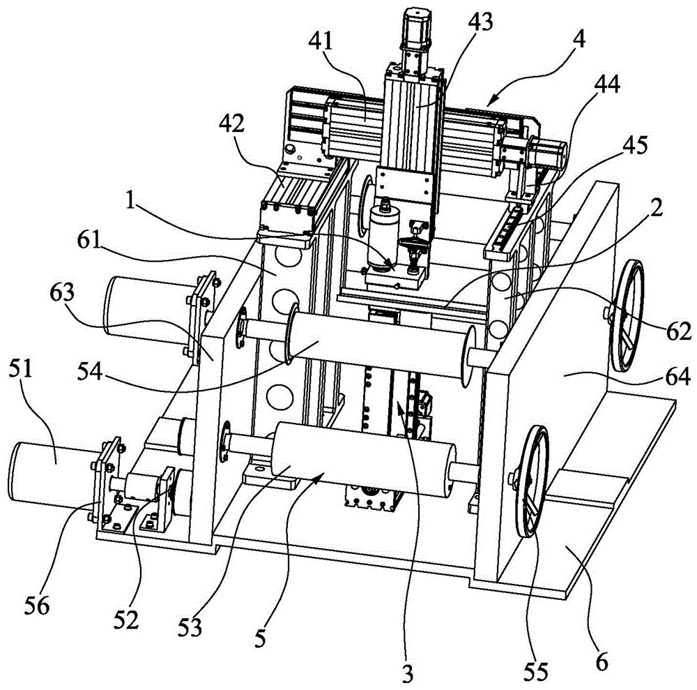
[0029] What the present invention discloses is a method for manufacturing a thin film transistor. The method uses micron and nanoscale droplet compound spraying technology on the base material, and sprays out each structural feature of the transistor layer by layer according to the structure and material of the thin film transistor, and when The nano-jet method is used when the characteristic size of the transistor is smaller than the micro-jet size or fine spray is required, otherwise the micro-jet method is used.

[0030] In order to realize the above method, the existing micro-jet device and nano-scale electrofluid jet device can be used for complex switching. However, due to the different principles, equipment and nozzle structures of existing micro-jet and nano-jet, the efficiency is low and the positioning is inaccurate when spr...


PUM


Abstract

The invention discloses a manufacturing method of a thin film transistor and a micro-nano composite spraying machine thereof. In the provided method, a micrometer and nanometer droplet composite spraying technology is adopted to spray electrodes, insulation layers or protective layers of a thin film transistor on a substrate material layer by layer according to the structure and materials of the thin film transistor. When the characteristic size of the transistor is smaller than the micrometer spraying size or a fine spraying mode is carried out, the nanometer spraying mode is adopted, or otherwise the micrometer spraying mode is adopted. An electric field is provided for the micro-nano composite spraying machine on the basis of pyroelectric effect so as to avoid to directly apply high voltage and complicated circuit on the nano spraying device, so the problems caused by the high voltage and complicated circuit are solved. Moreover, the provided composite spraying machine can efficiently spray on a large-surface electronic device, and the cost is low.

Description

technical field [0001] The invention relates to printed electronic technology, in particular to a manufacturing method of a thin film transistor and a micro-nano composite jetting machine. Background technique [0002] In the past ten years, the rapid development of the printed electronics industry has attracted great interest and attention from many researchers. Thanks to the rapid research progress of organic materials and the development of large-area, flexible, and low-cost printing processes, printed electronics technology is rapidly developing. Become a new industry that can compete with silicon-based microelectronics technology. However, the defects of low charge mobility of organic materials, low positioning accuracy and low resolution of traditional printed patterns seriously restrict the further development of printed electronics technology. Therefore, how to fabricate transistor devices with smaller feature size, higher precision and better performance at low cos...

Claims


Application Information

Patent Timeline
Patent Type & Authority Patents(China)
IPC IPC(8): B29C64/112B29C64/227B29C64/291B33Y30/00B33Y40/00B33Y10/00
Inventor 谢丹常雪峰舒霞云罗善明王建郑康
Owner XIAMEN UNIV OF TECH
Why Eureka
Try Eureka