Light emitting diode
A technology of light-emitting diodes and electrodes, applied in electrical components, circuits, semiconductor devices, etc., can solve the problems of less formation area, inability to effectively radiate recombination, and decrease in luminous intensity, so as to improve recombination efficiency, luminous efficiency, and luminous intensity. the effect of strength
- Summary
- Abstract
- Description
- Claims
- Application Information
AI Technical Summary
Problems solved by technology
Method used
Image

Examples
Embodiment Construction
[0064] In order to make the object, technical solution and advantages of the present invention clearer, the present invention will be further described in detail below in conjunction with specific embodiments and with reference to the accompanying drawings.
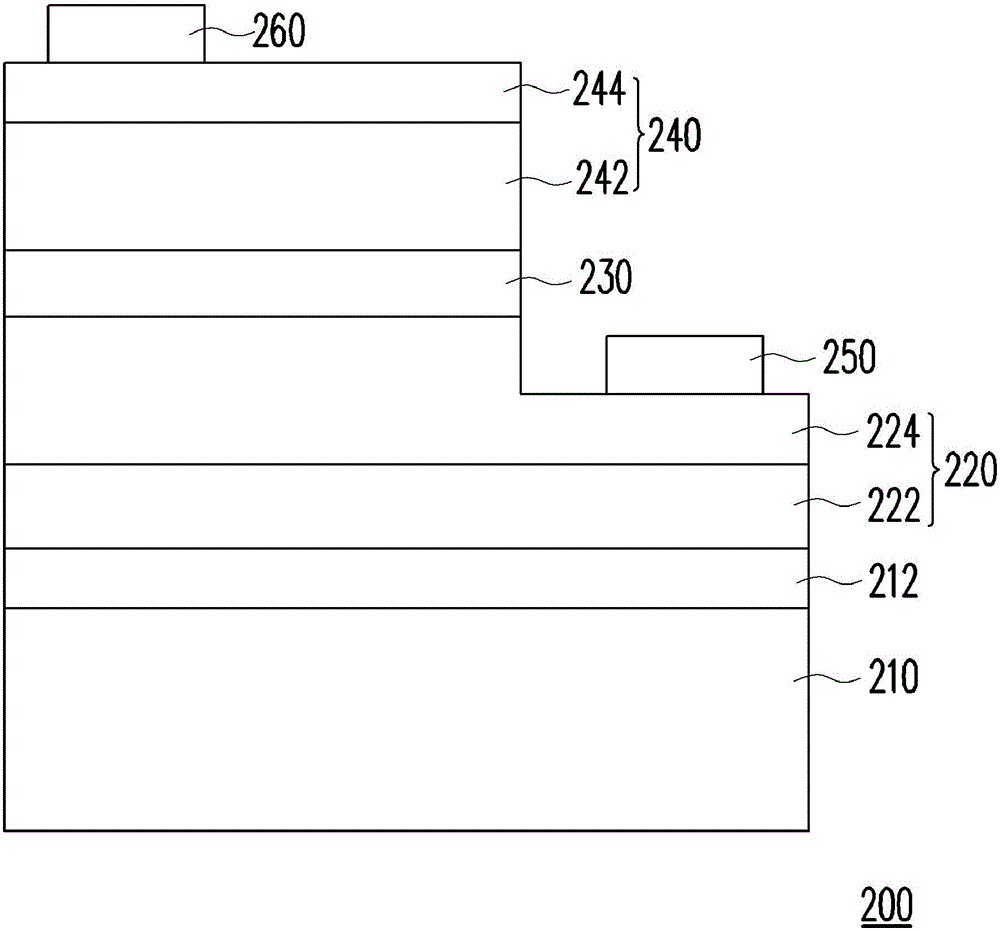
[0065] figure 1 It is a schematic cross-sectional view of a light emitting diode in an embodiment of the present invention.
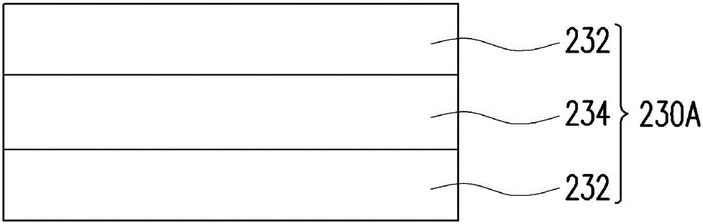
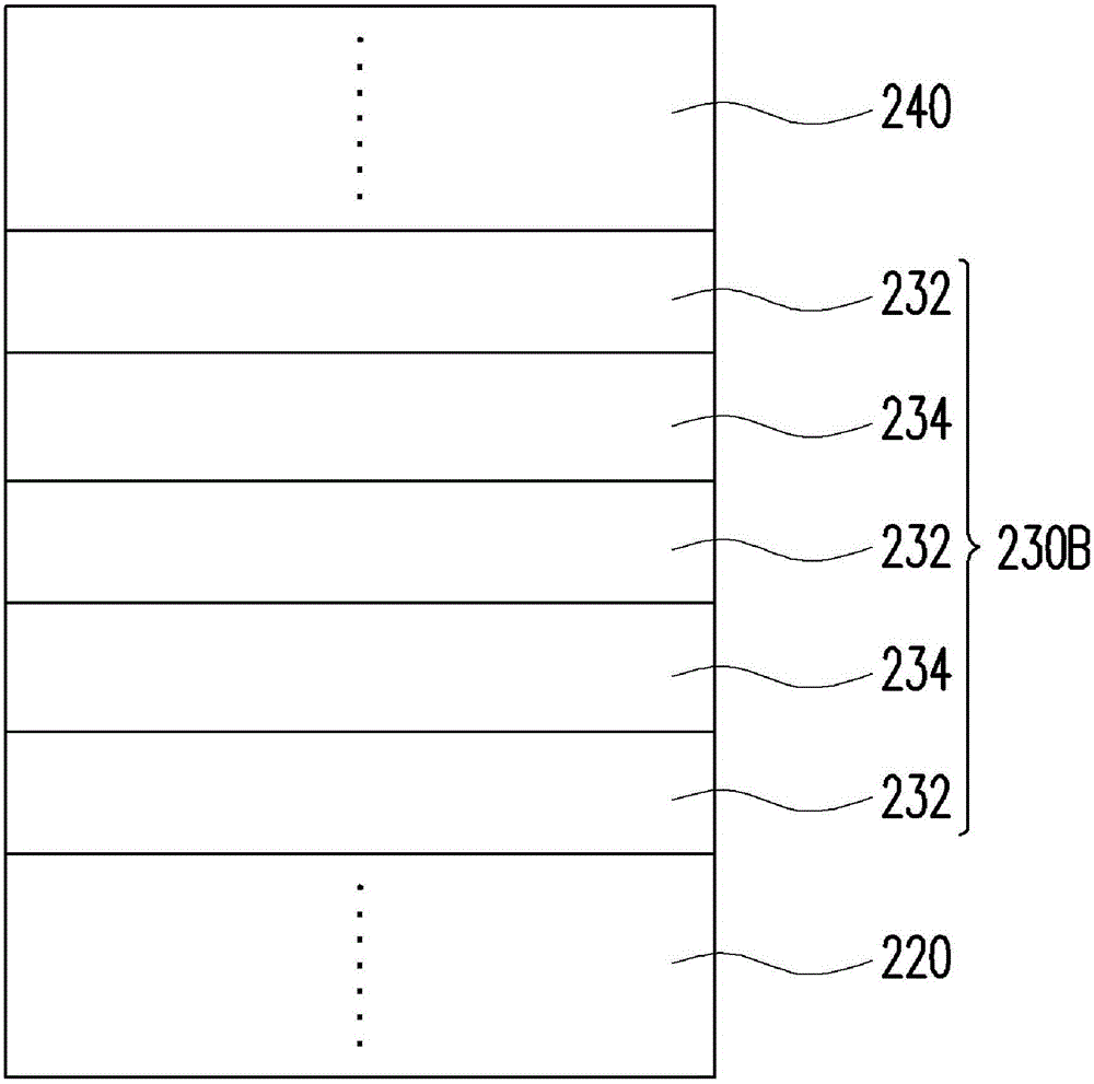
[0066] Please refer to figure 1 The LED 200 includes a substrate 210 , an N-type semiconductor layer 220 , an active layer 230 , a P-type semiconductor layer 240 , and a first electrode 250 and a second electrode 260 , and the substrate 210 is, for example, a sapphire substrate. Specifically, a nitride semiconductor coating layer 212 (for example, undoped gallium nitride), an N-type semiconductor layer 220, an active layer 230, and a P-type semiconductor layer 240 are sequentially formed on a surface of the sapphire substrate 210. The active layer 230 is located between the N-type semiconductor l...
PUM
| Property | Measurement | Unit |
|---|---|---|
| Light wavelength | aaaaa | aaaaa |
Abstract
Description
Claims
Application Information
 - Generate Ideas
- Intellectual Property
- Life Sciences
- Materials
- Tech Scout
- Unparalleled Data Quality
- Higher Quality Content
- 60% Fewer Hallucinations
Browse by: Latest US Patents, China's latest patents, Technical Efficacy Thesaurus, Application Domain, Technology Topic, Popular Technical Reports.
© 2025 PatSnap. All rights reserved.Legal|Privacy policy|Modern Slavery Act Transparency Statement|Sitemap|About US| Contact US: help@patsnap.com