Reaction chamber and semiconductor processing equipment

A technology of reaction chamber and magnetic conduction, which is applied in semiconductor/solid-state device manufacturing, plasma, metal material coating technology, etc., can solve the problems of substrate damage, reduction of available space, ignition process, etc., and achieve reduction Damage to the substrate, increase the available space, and improve the effect of process quality

Active Publication Date: 2015-11-25
BEIJING NAURA MICROELECTRONICS EQUIP CO LTD
View PDF7 Cites 14 Cited by
  • Summary
  • Abstract
  • Description
  • Claims
  • Application Information

AI Technical Summary

Problems solved by technology

[0006] One, since the surface of the metal deposition is the upper surface (i.e., the horizontal plane) of the insulating ring, this makes most of the metal particles downward (i.e., along the vertical direction) when the reaction chamber is exhausted from top to bottom. direction) movement, along with the progress of the process, the metal deposited on the upper surface of the insulating ring 17 is easy to cause the Faraday shielding ring 14 to conduct at the slot position of its lower surface, thereby causing the gap in the slot Sparking is prone to occur at the position, which will affect the process, and then affect the stability of the process; moreover, due to too much deposited metal, excessive metal peeling will cause particle pollution to the reaction chamber, thereby causing serious damage to the substrate;
[0007] Second, in order to avoid the conduction of the Faraday shielding ring 14, the size ratio of the recess 15 in the horizontal direction and the vertical direction of the reaction chamber is usually relatively high, but the thickness of the Faraday shielding ring 14 in its radial direction is relatively large , thus reducing the inner diameter of the reaction chamber and reducing the available space, which will affect the uniformity of the process

Method used


Image

  • Reaction chamber and semiconductor processing equipment
  • Reaction chamber and semiconductor processing equipment
  • Reaction chamber and semiconductor processing equipment

Examples


Embodiment Construction

[0030] In order for those skilled in the art to better understand the technical solutions of the present invention, the reaction chamber and semiconductor processing equipment provided by the present invention will be described in detail below with reference to the accompanying drawings.

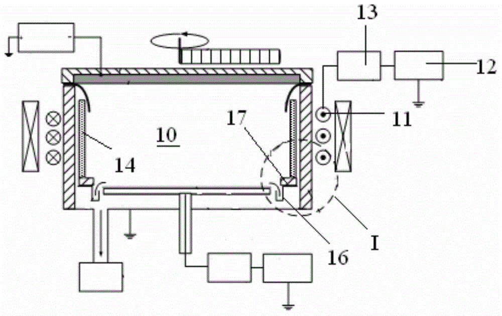
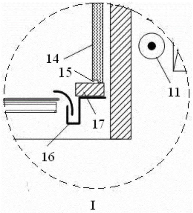
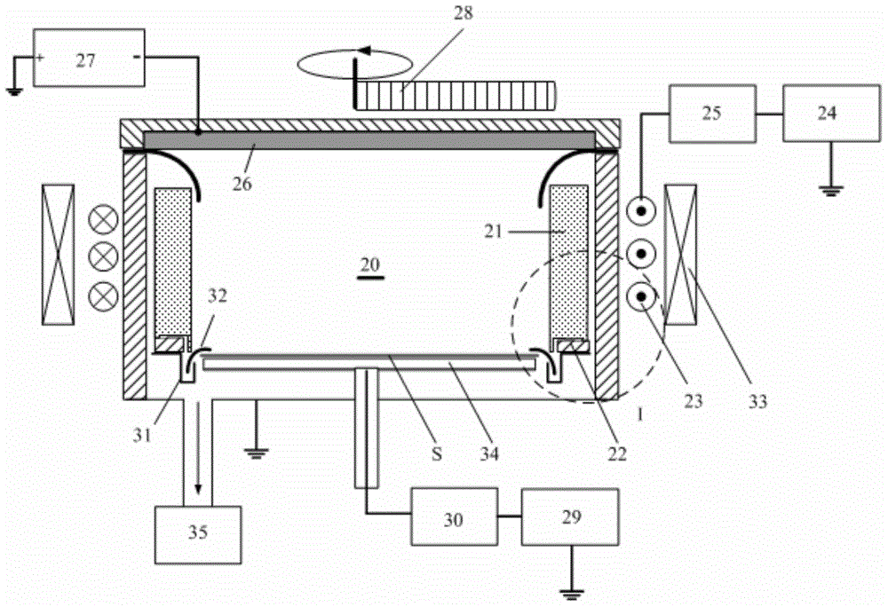
[0031] image 3 This is a schematic structural diagram of the reaction chamber provided in the embodiment of the present invention. Figure 4 for image 3 A zoomed-in view of region I in the middle. Figure 5 for image 3 Schematic diagram of the structure of the middle insulating ring and the Faraday shielding ring. Please also refer to image 3 , Figure 4 and Figure 5, the reaction chamber 20 provided in this embodiment includes a Faraday shielding ring 21, an insulating ring 22, an induction coil 23, a radio frequency power supply 24, a first impedance matcher 25, a target material 26, a DC power supply 27, a magnetron 28, a bias voltage The radio frequency power supply 29 , the ...


PUM


Abstract

A reaction chamber and semi-conductor processing device, comprising a Faraday shielding ring (21) made of nonconductive magnetic material and an insulating ring (22) made of insulating material; the Faraday shield ring (21) is provided with a slot thereon passing through the ring surface thereof in an axial direction; both the Faraday shielding ring (21) and the insulating ring (22) are disposed in the reaction chamber surrounding the inner peripheral wall of the reaction chamber; the Faraday shielding ring (21) is stacked on the insulating ring (22) in a vertical direction; a shielding ring (211) is disposed surrounding the inner peripheral wall of the insulating ring (22), the shielding ring (211) is connected to an area on the lower surface of the Faraday shielding ring (21) adjacent to the center of the reaction chamber; and the shielding ring (211) is made of the nonconductive magnetic material, and is provided with the slot thereon passing through the ring surface thereof in the axial direction. The reaction chamber and the semi-conductor processing device avoid or reduce the risk of sparking, reduce pollution of the reaction chamber caused by the flaking off of metal particles, and increase the inner diameter and available space of the reaction chamber.

Description

technical field [0001] The invention belongs to the technical field of semiconductor equipment manufacturing, and in particular relates to a reaction chamber and semiconductor processing equipment. Background technique [0002] Magnetron sputtering equipment is a widely used processing equipment, mainly used for the deposition process of substrates. The basic principle of magnetron sputtering is: the reaction gas is excited to form plasma, and the target 26 in the reaction chamber is bombarded by the plasma, so that various particles on the surface of the target 26 escape and deposit on the substrate. In the production of VLSI semiconductor devices, it is usually necessary to deposit metal layers in high aspect ratio channels, trenches or vias on the substrate surface, thus increasing the ion concentration in the plasma in the reaction chamber. [0003] For this, use figure 1 reaction chamber shown, see figure 1 and figure 2 , an induction coil 11 is arranged around the...

Claims


Application Information

Patent Timeline
Patent Type & Authority Applications(China)
IPC IPC(8): H01J37/32
CPCH01L21/00C23C14/564H01J37/32651H01J37/3405H01J37/3441C23C14/34H01J37/32H01L21/02631H01L21/203H05H1/46C23C14/14C23C14/35H01L21/2855
Inventor 张彦召佘清陈鹏
Owner BEIJING NAURA MICROELECTRONICS EQUIP CO LTD
Why Eureka
Try Eureka