Preparation method for memory cell of resistive random access memory and product thereof

A random access memory and storage unit technology, applied in the direction of electrical components, etc., can solve the problems of restricting the industrial production of RRAM, unfavorable RRAM compatibility, unfavorable practical application of storage devices, etc., and achieve the effect of eliminating the formation process of electricity, increasing the concentration, and reducing the initial resistance

Active Publication Date: 2015-11-25
NINGBO INST OF MATERIALS TECH & ENG CHINESE ACADEMY OF SCI
View PDF8 Cites 3 Cited by
  • Summary
  • Abstract
  • Description
  • Claims
  • Application Information

AI Technical Summary

Problems solved by technology

[0007] The existence of the electroforming process is detrimental to the practical application of memory devices
In addition, the existence of this electrical formation proc

Method used


Image

  • Preparation method for memory cell of resistive random access memory and product thereof
  • Preparation method for memory cell of resistive random access memory and product thereof
  • Preparation method for memory cell of resistive random access memory and product thereof

Examples


Embodiment 1

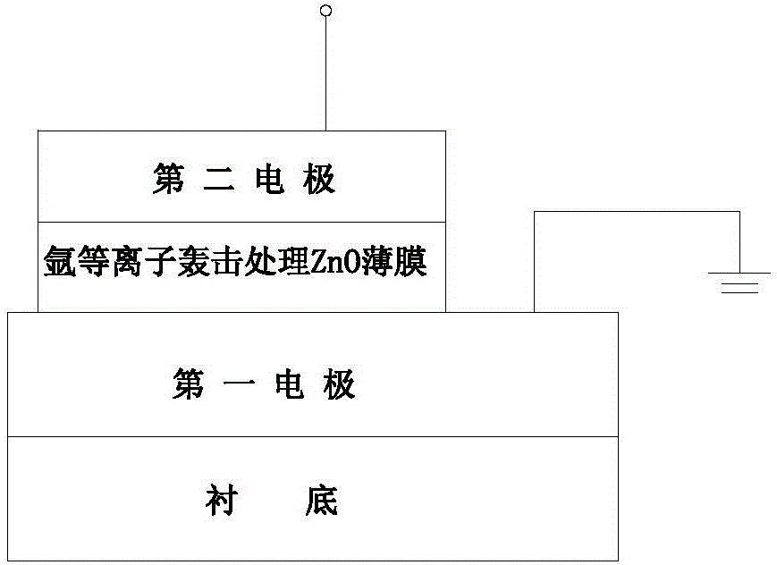
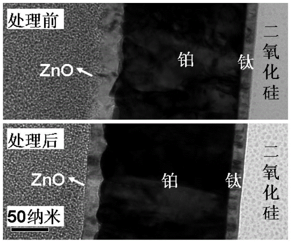
[0046] The storage unit of the resistive random access memory prepared in this embodiment includes an insulating substrate, the insulating substrate is composed of single crystal silicon and a silicon dioxide isolation dielectric layer grown on the surface of the single crystal silicon, and the silicon dioxide isolation dielectric layer is provided with a second One electrode, the first electrode is made up of titanium with a thickness of 20nm and platinum with a thickness of 150nm; the middle layer of ZnO thin film treated with argon plasma bombardment is arranged on the surface of the first electrode, the thickness of the middle layer is 20nm, and the surface of the middle layer is made of platinum The second electrode, the thickness of the second electrode is 50nm.

[0047]The preparation method of the storage unit of the above-mentioned resistance random access memory is:

[0048] Step 1, using a thermal oxidation method to grow a silicon dioxide isolation dielectric layer...

Embodiment 2

[0058] The storage unit of the resistive random access memory prepared in this embodiment includes an insulating substrate, the insulating substrate is composed of single crystal silicon and a silicon dioxide isolation dielectric layer grown on the surface of the single crystal silicon, and the silicon dioxide isolation dielectric layer is provided with a second One electrode, the first electrode is composed of 20nm thick titanium and 150nm thick platinum; the middle layer of the ZnO thin film treated with argon plasma bombardment is arranged on the surface of the first electrode, the thickness of the middle layer is 21nm, and the surface of the middle layer is made of copper The second electrode, the thickness of the second electrode is 50nm.

[0059] The preparation method of the storage unit of the above-mentioned resistance random access memory is:

[0060] Step 1, using a thermal oxidation method to grow a silicon dioxide isolation dielectric layer on the single crystal s...


PUM

PropertyMeasurementUnit
Thicknessaaaaaaaaaa
Thicknessaaaaaaaaaa
Thicknessaaaaaaaaaa

Abstract

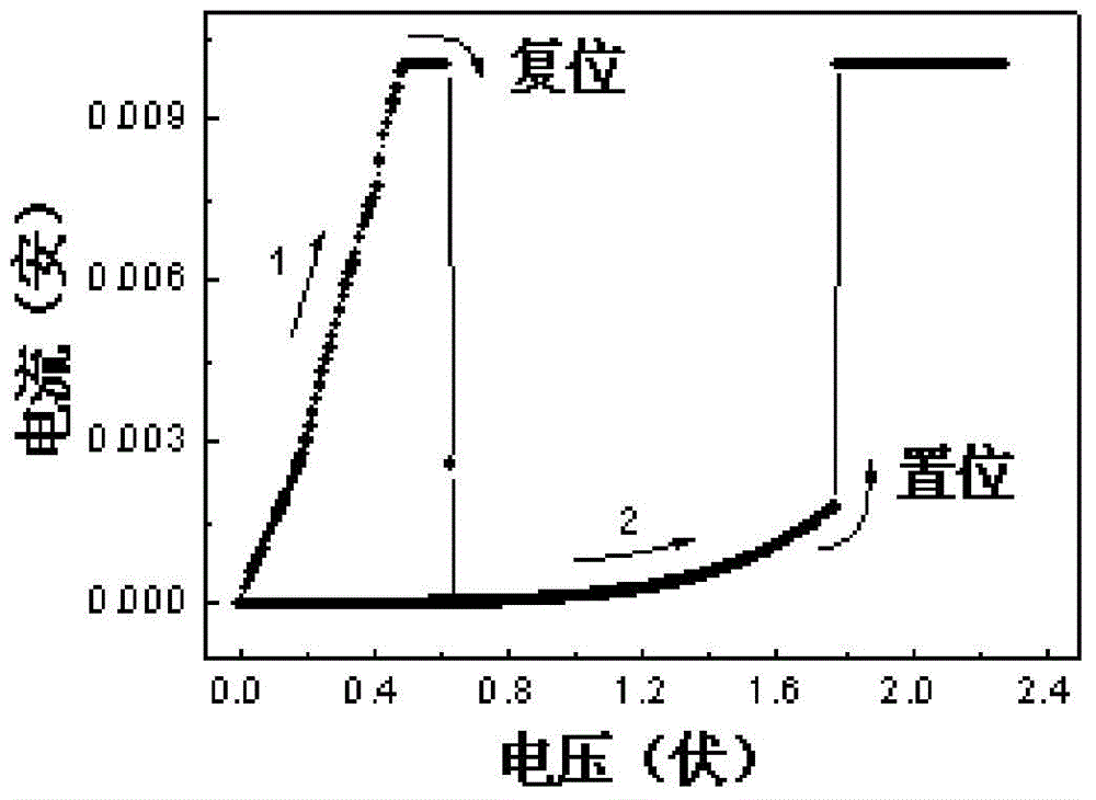
The invention discloses a preparation method for a memory cell of a resistive random access memory. The method includes: step 1, a conductive film as a first electrode is formed on the surface of a substrate; step 2, a ZnO film through argon plasma bombardment treatment as an intermediate layer is prepared on the surface of the first electrode obtained by the step 1; step 3, a conductive film as a second electrode is prepared on the surface of the intermediate layer obtained by the step 2; and step 4, an isolation device is prepared on the structural basis obtained by the step 3, and the memory cell of the resistive random access memory is obtained. According to the preparation method for the memory cell of the resistive random access memory, the argon plasma bombardment treatment of the ZnO film as the intermediate medium layer is performed so that the flatness of the surface of the ZnO film is greatly improved; and the ZnO film through argon plasma bombardment treatment serves as the memory prepared by the intermediate layer, the initial presentation is the low-resistance state, the wiping of all the devices does not need the process of electric forming, and the wiping voltage is low.

Description

technical field [0001] The invention relates to the technical field of non-volatile memory, in particular to a method for preparing a storage unit of a resistance random access memory and a product thereof. Background technique [0002] The current rapid development of digital high-tech has put forward higher requirements for the performance of existing information storage products, such as: high speed, high density, long life, low cost and low power consumption, etc. technical deficiencies. One of the weaknesses of dynamic and static memory is its volatility: information is lost in the event of a power outage, and it is susceptible to interference from electromagnetic radiation. Flash memory has technical obstacles such as slow read and write speeds and low recording density. Therefore, breakthroughs in storage materials and technologies are urgently needed to develop new-generation memory technologies. [0003] In 2000, the University of Houston in the United States dis...

Claims


Application Information

Patent Timeline
IPC IPC(8): H01L45/00
Inventor 诸葛飞伏兵曹鸿涛
Owner NINGBO INST OF MATERIALS TECH & ENG CHINESE ACADEMY OF SCI
Why Eureka
Try Eureka