

A preparation method and product of a storage unit of a resistive random access memory
A technology of random access memory and storage unit, applied in the direction of electrical components, etc., can solve the problems of restricting the industrial production of RRAM, unfavorable practical application of storage devices, unfavorable RRAM compatibility, etc., and achieve the effect of eliminating the formation process of electricity, increasing the concentration, and reducing the initial resistance
- Summary
- Abstract
- Description
- Claims
- Application Information
AI Technical Summary
Problems solved by technology
Method used
Image

Examples
Embodiment 1
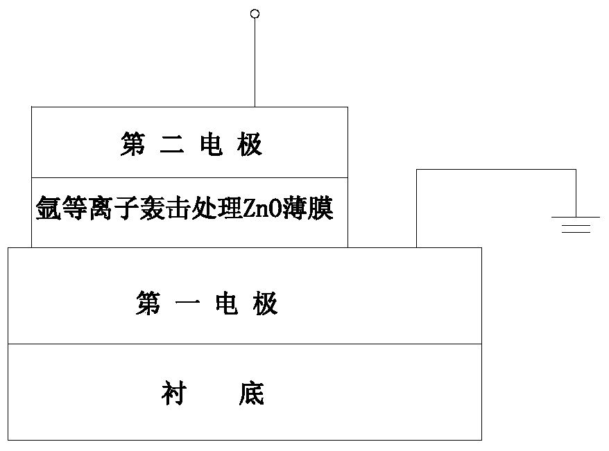
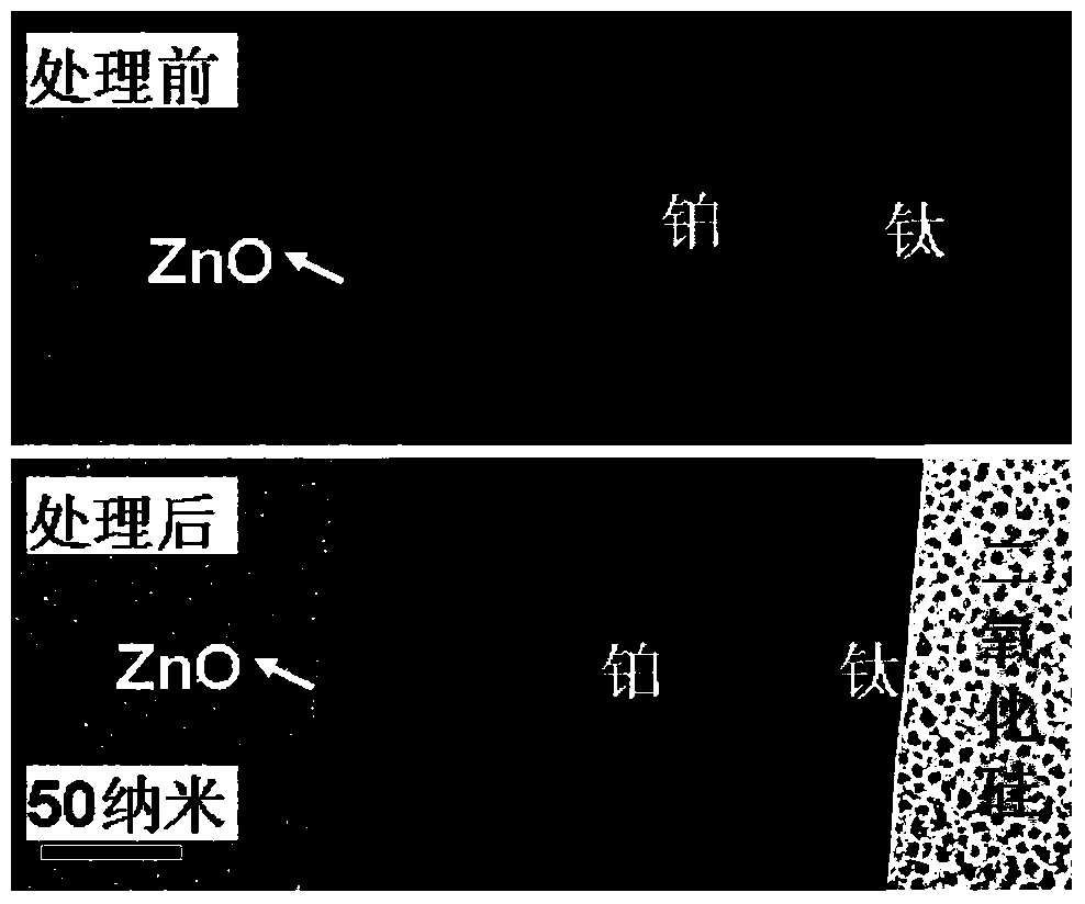
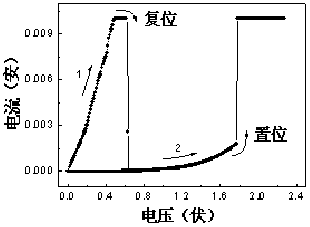
[0046] The storage unit of the resistive random access memory prepared in this embodiment includes an insulating substrate, the insulating substrate is composed of single crystal silicon and a silicon dioxide isolation dielectric layer grown on the surface of the single crystal silicon, and the silicon dioxide isolation dielectric layer is provided with a second One electrode, the first electrode is made up of titanium with a thickness of 20nm and platinum with a thickness of 150nm; the middle layer of ZnO thin film treated with argon plasma bombardment is arranged on the surface of the first electrode, the thickness of the middle layer is 20nm, and the surface of the middle layer is made of platinum The second electrode, the thickness of the second electrode is 50nm.
[0047]The preparation method of the storage unit of the above-mentioned resistance random access memory is:
[0048] Step 1, using a thermal oxidation method to grow a silicon dioxide isolation dielectric layer...
Embodiment 2
[0058] The storage unit of the resistive random access memory prepared in this embodiment includes an insulating substrate, the insulating substrate is composed of single crystal silicon and a silicon dioxide isolation dielectric layer grown on the surface of the single crystal silicon, and the silicon dioxide isolation dielectric layer is provided with a second One electrode, the first electrode is composed of 20nm thick titanium and 150nm thick platinum; the middle layer of the ZnO thin film treated with argon plasma bombardment is arranged on the surface of the first electrode, the thickness of the middle layer is 21nm, and the surface of the middle layer is made of copper The second electrode, the thickness of the second electrode is 50nm.
[0059] The preparation method of the storage unit of the above-mentioned resistance random access memory is:
[0060] Step 1, using a thermal oxidation method to grow a silicon dioxide isolation dielectric layer on the single crystal s...
PUM
| Property | Measurement | Unit |
|---|---|---|
| thickness | aaaaa | aaaaa |
| thickness | aaaaa | aaaaa |
| thickness | aaaaa | aaaaa |
Abstract
Description
Claims
Application Information