An optical readout infrared detector structure and its manufacturing method
An infrared detector, optical readout technology, applied in optical radiation measurement, scientific instruments, microstructure technology, etc., can solve the problem of not being able to meet the mechanical strength at the same time, to improve the utilization rate of infrared radiation, ensure safe release, and avoid heat The effect of crosstalk
- Summary
- Abstract
- Description
- Claims
- Application Information
AI Technical Summary
Problems solved by technology
Method used
Image
Examples
Embodiment 1
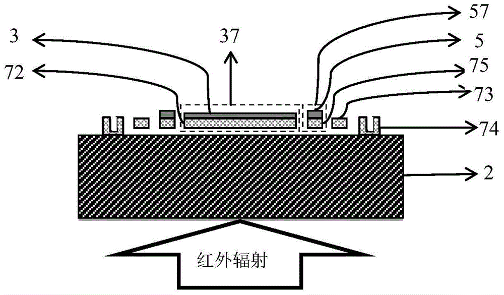
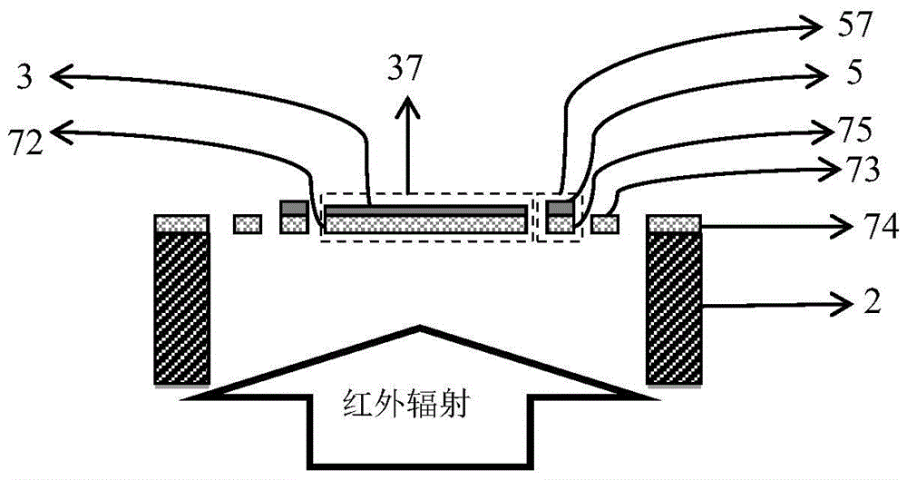
[0077] This embodiment provides an optical readout infrared detector structure, please refer to the attached Figure 3i , attached Figure 4j , attached Figure 5 And attached Image 6 , the infrared detector structure at least includes: a glass substrate 1 and a suspension structure, the suspension structure is suspended on the glass substrate 1 through the second anchor 74 . The suspended structure includes a visible light reflecting layer 3, an infrared absorbing layer 72 and a support beam; the visible light reflecting layer 3 is suspended on the glass substrate 1, and the infrared absorbing layer 72 is suspended above the visible light through a first anchor 71. On the reflective layer 3, the support beam is suspended on the visible light reflective layer 3, and one end of the support beam is connected to the infrared absorbing layer 72 in the same plane, and the other end is fixed to the on a glass substrate 1.
[0078] It should be noted, Figure 3i with 4j yes ...
Embodiment 2
[0084] This embodiment provides a method for fabricating an optical readout infrared detector structure, please refer to the attached Figure 3a-3i , for making the optical readout infrared detector structure in Embodiment 1, the specific implementation steps are as follows:
[0085] First perform step 1, such as Figure 3a~3b As shown, a silicon substrate 2 is provided as a sacrificial substrate, and a glass substrate 1 is provided, the sacrificial substrate is bonded to the glass substrate 1, and the sacrificial substrate is thinned to form a first sacrificial layer twenty one.
[0086] In this step, the silicon substrate 2 is a double-throw silicon wafer, and the glass substrate 1 is a double-throw glass wafer.
[0087] The specific process of this step is:
[0088] (1) Perform anodic bonding of double-polished silicon wafers and double-polished glass wafers at a bonding temperature of 200-450°C and a bonding voltage of 600-1400V, such as Figure 3a shown;
[0089] (2)...
Embodiment 3
[0111] This embodiment additionally provides a method for fabricating an optical readout infrared detector structure, please refer to the appended Figure 4a~4j , for making the optical readout infrared detector structure in Embodiment 1, the specific implementation steps are as follows:
[0112] Wherein step one to step three are the same as embodiment two, corresponding to the attached Figure 4a-4e , which will not be repeated here.
[0113] Then perform step 4, such as Figure 4f As shown, the second sacrificial layer 4 and the first sacrificial layer 21 are etched to form the second anchor region 6 exposing the glass substrate 1 .
[0114] The second sacrificial layer 4 and the first sacrificial layer 21 are etched using a deep reactive ion etching (DRIE) technique to form a second anchor region 6 exposing the surface of the glass substrate 1 .
[0115] In addition to the deep reactive ion etching technology, other suitable etching methods can also be used to etch the ...
PUM
| Property | Measurement | Unit |
|---|---|---|
| thickness | aaaaa | aaaaa |
| thickness | aaaaa | aaaaa |
| thickness | aaaaa | aaaaa |
Abstract
Description
Claims
Application Information


