Method for depositing film through high ionization rate high power pulse magnetron sputtering

A high-power pulse and magnetron sputtering technology, which is applied in sputtering plating, ion implantation plating, metal material coating technology, etc., can solve problems such as uneven bonding force, non-dense and poor film, and achieve Uniform binding force, improved ionization rate, high binding force effect

Active Publication Date: 2015-12-16
SOUTH CHINA UNIV OF TECH
View PDF5 Cites 18 Cited by
  • Summary
  • Abstract
  • Description
  • Claims
  • Application Information

AI Technical Summary

Problems solved by technology

[0007] The purpose of the present invention is to provide a high ionization rate high power pulse magnetron sputtering in order to solve the problems of non-dense, uneven and poor bonding force of the film caused by the low ionization rate of the existing high power pulse. film deposition method

Method used


Image

  • Method for depositing film through high ionization rate high power pulse magnetron sputtering
  • Method for depositing film through high ionization rate high power pulse magnetron sputtering
  • Method for depositing film through high ionization rate high power pulse magnetron sputtering

Examples


Embodiment 1

[0040] This embodiment is a method for depositing a thin film by high ionization rate and high power pulse magnetron sputtering, which is specifically carried out according to the following steps:

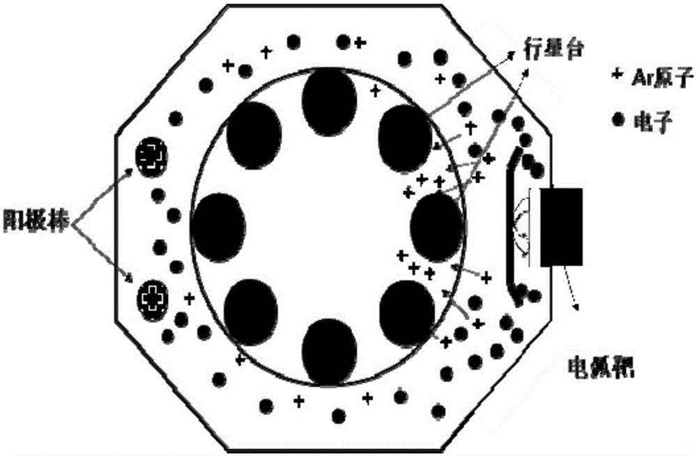
[0041] 1) Ti metal is selected as the target material, and the M2 high-speed steel sample cleaned by acetone alcohol ultrasonic cleaning is dried, fixed on a three-dimensionally rotatable planetary table, and placed in a cleaned vacuum chamber. The target base distance is 10cm;

[0042] 2) Seal the vacuum chamber, and use high-purity Ar gas to pump the chamber to a background vacuum of 4×10 through a mechanical pump and a molecular turbo pump. -5 mbar, and then set the infrared electric heating tube to heat at 600°C to remove moisture on the surface of the sample and adsorb air impurities;

[0043] 3) The vacuum is stable at 4×10 -5 After mbar, the infrared electric heating tube is set to 500°C, the sample is applied with a negative bias voltage of 300V, the pulse frequency is 20...

Embodiment 2

[0056] The difference between this embodiment and specific embodiment 1 is that the commercially available ground YT14 is selected as the test material, the roughness is 144nm, and the Vickers hardness is 1725HV 0.2 , others are identical with embodiment 1.

[0057] Brief results of this example:

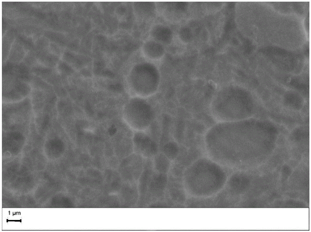
[0058] The surface morphology of the ground YT14 cemented carbide after coating by the above-mentioned high-ionization rate high-power pulse magnetron sputtering method is shown in Fig. Figure 7 , its surface hardness is 1725HV 0.2 , the thickness is about 300nm~500nm, and the film-base bonding interface is dense, see Figure 8 .

[0059] The ground YT14 cemented carbide has an original roughness of 144nm. During the coating process, due to the bombardment of Ar+ and the deposition of the film layer, the roughness becomes 240nm. The rating results of the indentation method are shown in Figure 9 .

Embodiment 3

[0061] The difference between this embodiment and Example 1 is that the commercially available polished nano-hard alloy is selected as the test material, and its composition mass fraction is C0.84%, W84.64%, Cr1.34%, Co13.18%, Roughness is 240nm, Vickers hardness is 1787HV 0.2 , probably because the indenter is pressed too deeply, showing a composite Vickers hardness. Others are the same as in Example 1.

[0062] Brief results of this implementation:

[0063] The surface morphology of the polished nano-hard alloy after coating by the above-mentioned high-ionization rate high-power pulse magnetron sputtering method is shown in Fig. Figure 10 , its surface hardness is 1787HV 0.2 Increase to 2056HV 0.2 , the thickness is about 700nm~1000nm,.

[0064] The polished nano-hard alloy has an original roughness of 240nm. During the coating process, due to the bombardment of Ar+ and the deposition of the film, the roughness becomes 62nm. It can be seen that the film particles are v...


PUM

PropertyMeasurementUnit
hardnessaaaaaaaaaa
hardnessaaaaaaaaaa
hardnessaaaaaaaaaa

Abstract

The invention discloses a method for depositing a film through high ionization rate high power pulse magnetron sputtering, relates to the technical field of film materials, and mainly solves the problems that the existing target is low in ionization rate, the plasma is nonuniform and the film uniformity is poor. The method comprises the following steps: I, cleaning a chamber, and fixing a test sample on a planet platform; II, placing the planet platform in the sealed chamber, vacuumizing the chamber, and removing moisture on the test sample and absorbed air; III, applying back bias voltage on the test sample, and feeding high-purity Ar; IV, feeding Ar and N2 in the chamber, and applying impulse voltage on a sputtering target for surface coating; V, adopting a stepping motor to control the motion track of the planet platform so as to control film coating; VI, taking the test sample out when the temperature in the vacuum chamber is reduced to the room temperature. According to the invention, target magnetic field control during film preparation and target voltage applying form during film coating are changed, so that the film thickness and density are easy to control, and the binding force and the uniformity are high.

Description

technical field [0001] The invention relates to the technical field of thin film materials, in particular to a method for depositing thin films by high ionization rate and high power pulse magnetron sputtering. Background technique [0002] High-power pulsed magnetron sputtering technology is a newly developed coating technology in recent years. Its main features are its high peak power density, high substrate current density, high target ionization rate, low pulse frequency and duty cycle, which can realize the control of thin film Microstructure, reduce the internal stress of the film, control the phase structure of the film, etc. High-power pulsed magnetron sputtering has a high particle ionization rate, and the metal ions produced by collision with high-energy electrons have high energy. When the high-energy ions fly to the substrate, a large amount of energy will be bombarded and transferred to the substrate. Then it has an important impact on the surface state, qualit...

Claims


Application Information

Patent Timeline
Patent Type & Authority Applications(China)
IPC IPC(8): C23C14/35C23C14/02
Inventor 匡同春李雪萍蔡盼盼邓阳谭超林周克崧
Owner SOUTH CHINA UNIV OF TECH
Why Eureka
Try Eureka