MEMS metal-oxide semiconductor gas sensor and manufacturing method thereof

An oxide semiconductor and gas sensor technology, applied in instruments, scientific instruments, measuring devices, etc., can solve the problems of poor slurry stability, difficult automation of the process, low sensitivity, etc., and achieves low mass manufacturing cost, good product consistency, The effect of a high degree of automation

Inactive Publication Date: 2015-12-16
武汉微纳传感技术有限公司
View PDF0 Cites 38 Cited by
  • Summary
  • Abstract
  • Description
  • Claims
  • Application Information

AI Technical Summary

Problems solved by technology

At present, ceramic tubular gas sensors are the most widely used in the market, but their products are large in size, high in power consumption, low in sensitivity, and slow in response recovery time. Part of the product manufacturing process is difficult to automate, resulting in high manufacturing costs and limiting its application.
With the advancement of MEMS technology, several companies have begun to introduce commercial MEMS metal oxide semiconductor gas sensors in the past ten years, and gradually began mass production. However, these gas sensor sensitive material films generally use micron solid particles, nanometer solid Particles (doped with precious metal materials if necessary), except for a few special gases, the product sensitivity is still mainly at the ppm level (such as figure 1 As shown), air quality monitoring cannot be realized, and the accuracy of indoor air quality detection is not high
In recent years, many scientific research papers have published reports on the use of hollow nanotubes, hollow nanospheres and other nanostructures to improve the sensitivity of gas sensors, but there are few commercial products, mainly because these hollow nanostructure materials exist in process integration. More difficult, poor slurry stability, poor product consistency, poor film adhesion of sensitive materials, prone to defects such as falling off, difficult to effectively apply to products
[0003] Based on the above technical problems, the present invention provides a MEMS metal oxide semiconductor gas sensor and its manufacturing method, through the combination of hollow nanostructure materials, solid nanostructure materials, doped noble metal materials (when necessary), and the use of unique suspension Liquid ink formula and coating treatment process solve the problems in process integration

Method used


Image

  • MEMS metal-oxide semiconductor gas sensor and manufacturing method thereof
  • MEMS metal-oxide semiconductor gas sensor and manufacturing method thereof
  • MEMS metal-oxide semiconductor gas sensor and manufacturing method thereof

Examples


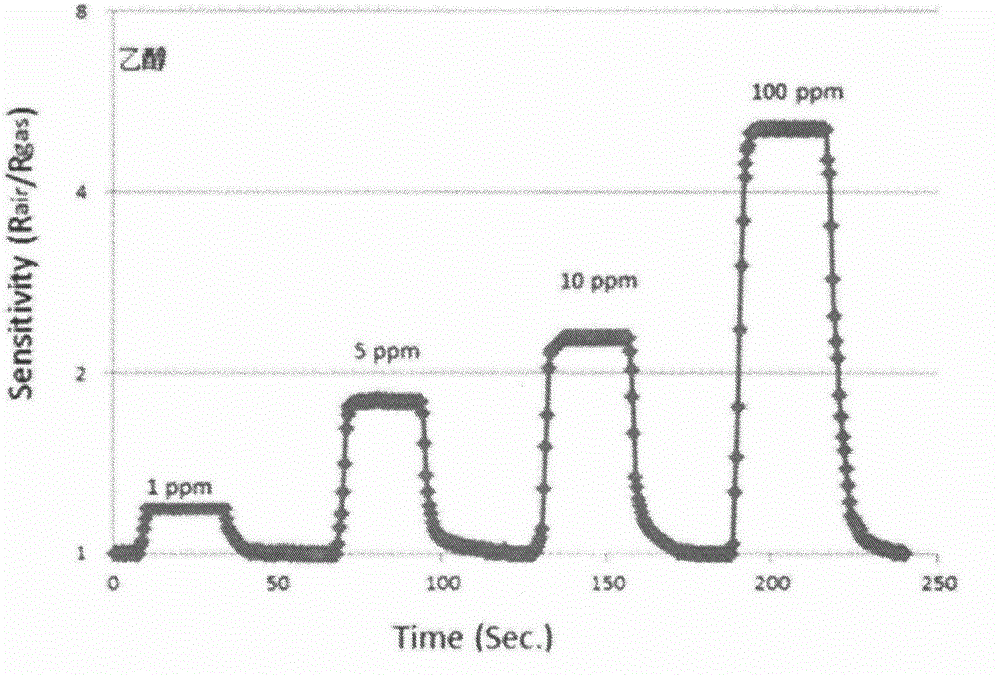
specific Embodiment 1

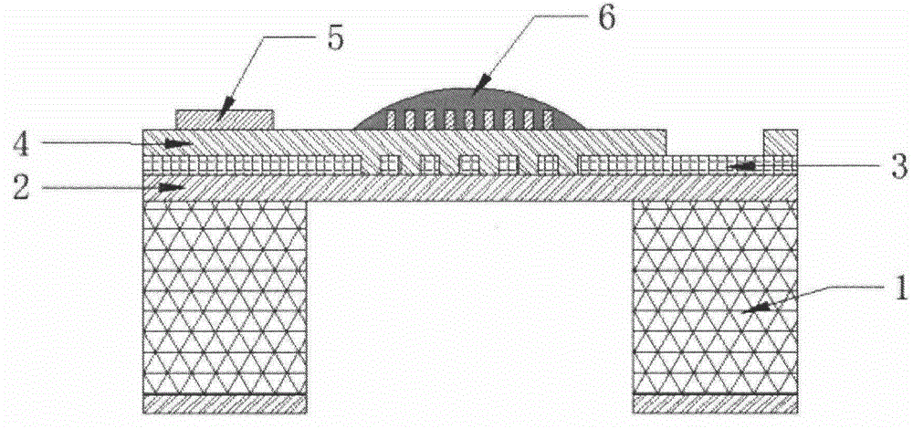
[0030] like figure 2 As shown, the present invention provides a kind of MEMS metal oxide semiconductor gas sensor, and this MEMS metal oxide semiconductor gas sensor comprises MEMS micro-hot plate, and described MEMS micro-hot plate comprises annular monocrystalline silicon substrate 1, supporting layer 2, heating An electrode 3, an insulating layer 4, a sensitive electrode 5, and a sensitive material film 6 coated in the measurement area of ​​the sensitive electrode.

[0031] Wherein, the annular single crystal silicon substrate 1 is formed by photolithography and dry ICP anisotropic etching process on the back of a single crystal silicon wafer. The supporting layer (2) is LPCVDSi 3 N 4formed with a thickness of 500 nm. The heating electrode (3) is Ta20nm / Pt200nm, formed by Liftoff process. The insulating layer (4) is composed of PECVDSiN with a thickness of 500nm. The sensitive electrode (5) is Ta20nm / Pt200nm, formed by sputtering and photolithography. The sensitive m...

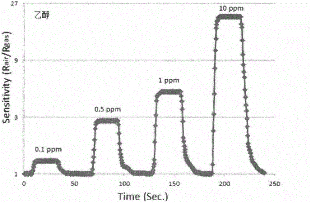
specific Embodiment 2

[0042] Next, a second embodiment of the present invention will be described with reference to the drawings.

[0043] like figure 2 As shown, the MEMS metal oxide semiconductor gas sensor includes a MEMS micro-hot plate, and the MEMS micro-hot plate includes an annular single crystal silicon substrate 1, a support layer 2, a heating electrode 3, an insulating layer 4, a sensitive electrode 5, and a coating Sensitive material film 6 in the sensitive electrode measurement area.

[0044] Wherein, the annular single crystal silicon substrate 1 is formed by photolithography and dry ICP anisotropic etching process on the back of a single crystal silicon wafer. The support layer 2 is LPCVDSi 3 N 4 formed with a thickness of 450 nm. The heating electrode 3 is Ti20nm / Pt200nm, formed by Liftoff process. The insulating layer 4 is composed of PECVDSiN with a thickness of 450nm. The sensitive electrode 5 is Ti20nm / Pt200nm, formed by Liftoff process. The sensitive material film 6 is ...


PUM

PropertyMeasurementUnit
sizeaaaaaaaaaa
thicknessaaaaaaaaaa
thicknessaaaaaaaaaa

Abstract

The invention provides an MEMS metal-oxide semiconductor gas sensor and a manufacturing method thereof. A sensitive material thin film is made of a hollow nanostructure material which includes at least one sort of metallic oxide. The manufacturing method includes the following steps that (a) an MEMS gentle heating disk is formed by the adoption of a semiconductor technology; (b) the hollow nanostructure material is synthesized through a hydrothermal method, and a solid nanostructure material is obtained through the methods of hydro-thermal synthesis, grinding and the like; (c) the hollow nanostructure material, the solid nanostructure material and a plurality of functional additives are prepared into slurry according to a certain proportion, and stable suspension liquid ink is obtained by means of stirring and ultrasonic dispersion; (d) the suspension liquid ink is printed in a sensitive electrode measuring area of the MEMS gentle heating disk; (e) low-temperature drying and high-temperature sintering are carried out, and accordingly the MEMS metal-oxide semiconductor gas sensor of a stable and reliable structure is formed. The MEMS metal-oxide semiconductor gas sensor has the advantages of being small in size, low in power consumption, high in sensitivity, short in response time, long in service life, capable of being integrated easily and the like.

Description

technical field [0001] The invention relates to the technical field of a metal oxide semiconductor gas sensor and its manufacture, in particular to a MEMS (Micro-Electro-Mechanic System) metal oxide semiconductor gas sensor and a manufacturing method thereof. Background technique [0002] In addition to traditional household gas leakage alarms and indoor air quality monitoring, the new MEMS metal oxide semiconductor gas sensors can also be potentially applied to portable detectors, wearable devices, smart phones, and Internet of Things air quality monitoring. At present, ceramic tubular gas sensors are the most widely used in the market, but their products are large in size, high in power consumption, low in sensitivity, and slow in response recovery time. Part of the product manufacturing process is difficult to automate, resulting in high manufacturing costs and limiting its application. With the advancement of MEMS technology, several companies have begun to introduce com...

Claims


Application Information

Patent Timeline
Patent Type & Authority Applications(China)
IPC IPC(8): G01N27/00
Inventor 雷鸣
Owner 武汉微纳传感技术有限公司
Why Eureka
Try Eureka