Packaging structure and packaging technology of high-voltage and high-power silicon carbide diodes

A silicon carbide diode and packaging structure technology, which is applied to semiconductor/solid-state device parts, semiconductor devices, electrical components, etc., can solve the problems of low chip welding reliability, large leakage of plastic packaging, and low dissipation loss, etc. Long-term reliability, low line loss, and effect of reducing heat loss

Active Publication Date: 2018-12-18
济南市半导体元件实验所
View PDF5 Cites 0 Cited by
  • Summary
  • Abstract
  • Description
  • Claims
  • Application Information

AI Technical Summary

Problems solved by technology

[0004] Aiming at the defects of the prior art, the present invention provides a high-voltage and high-power silicon carbide diode packaging structure and packaging process, which solves the problems of low chip welding reliability, large leakage of plastic packaging, and low dissipation loss in the prior art, and improves product quality. reliability

Method used


Image

  • Packaging structure and packaging technology of high-voltage and high-power silicon carbide diodes
  • Packaging structure and packaging technology of high-voltage and high-power silicon carbide diodes
  • Packaging structure and packaging technology of high-voltage and high-power silicon carbide diodes

Examples


Embodiment Construction

[0021] The present invention will be further described and limited below in conjunction with the accompanying drawings and specific embodiments.

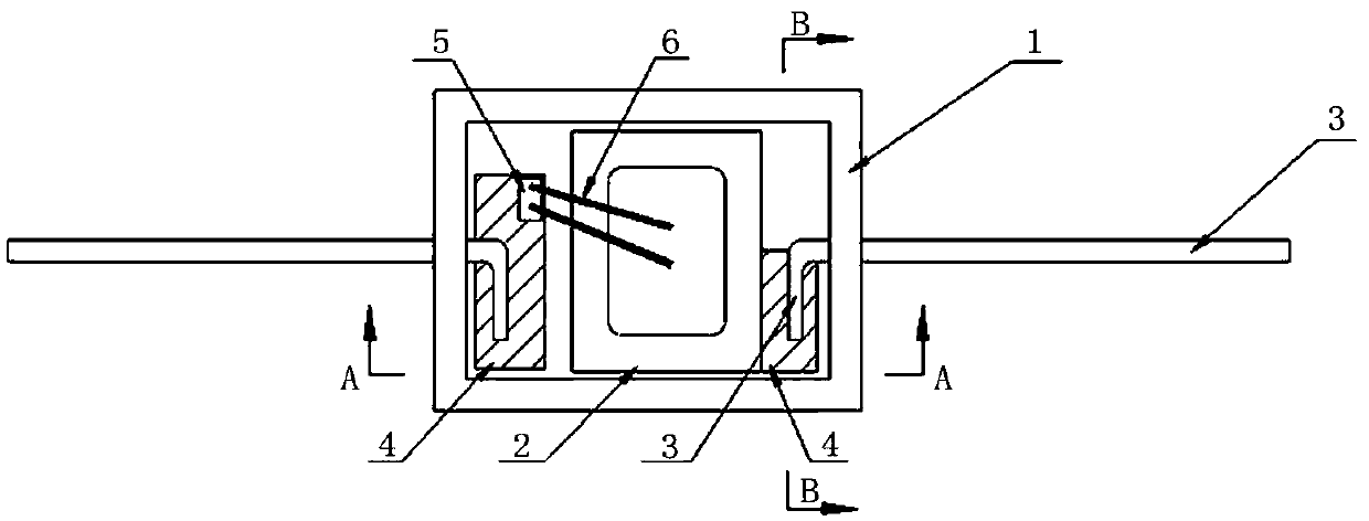
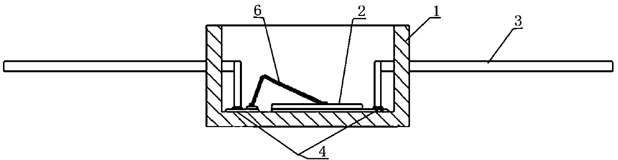
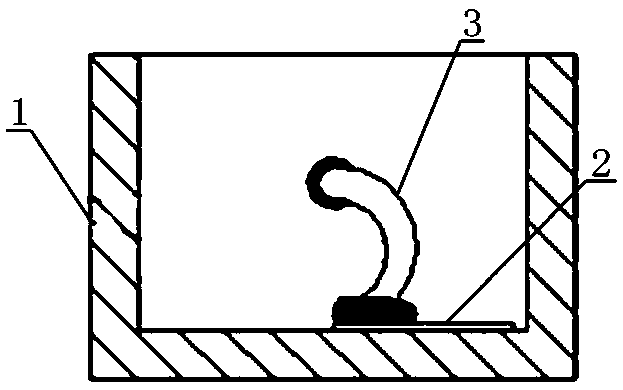
[0022] like figure 1 , 2 , 3, a high-voltage and high-power silicon carbide diode packaging structure, including a casing 1, a chip 2 located in the casing 1, and leads 3 connected to both ends of the casing 1, the casing 1 is a ceramic casing, and the chip 2 is welded to the ceramic casing. On the inner bottom surface of the casing 1, a conducting strip 4 is provided on both sides of the chip 2. The leads 3 at both ends of the casing are welded on the conducting strip 4. One of the conducting strips 4 is welded with a transition piece 5, and the transition piece 5 and the chip electrode are connected. The electrical connection is completed through the bonding wire 6.

[0023] In this embodiment, the casing 1 is a rectangular parallelepiped ceramic casing, and the chip 2 is directly welded to the inner bottom surface of the cerami...


PUM


Abstract

The invention discloses a high-voltage and high-power silicon carbide diode package structure and package process. The diode package structure comprises a shell, one or more chips and leads, wherein the chips are arranged in the shell and connected in series, the leads are connected to the two ends of the shell, the shell is a ceramic shell, the chips are welded on the inner bottom surface of the ceramic shell, the two sides of each chip are respectively provided with a guide tape, the leads at the two ends of the shell both are welded on the guide tapes, a transition sheet is welded on one of the guide tapes, and electrical connection between the transition sheet and a chip electrode is completed through a bonding wire. The package process adopts processes of chip vacuum welding, bonding wire ultrasonic bonding and the like, the diode has the advantages of high strength, low electric leakage, high reliability and the like, and the working temperatures of the chips are low.

Description

technical field [0001] The invention relates to a diode packaging structure and packaging process, in particular to a high-voltage and high-power silicon carbide diode packaging structure and packaging process, and belongs to the technical field of ceramic shell diode packaging. Background technique [0002] Silicon carbide Schottky diodes have zero reverse recovery time and switch speeds of up to 1MHz, because of their unique barrier structure, it is easy to achieve a high back voltage of tens of thousands of volts. At present, domestic institutes have developed SiC Schottky diodes with a voltage of 10kV and a current of 10A. However, due to the special properties of the product such as high voltage and high current, the packaging structure of traditional diodes cannot be directly applied, and the following packaging problems need to be faced. [0003] The size of the diode chip is about 10mm×10mm, and the chip area is large, so the problem of welding reliability must be ...

Claims


Application Information

Patent Timeline
Patent Type & Authority Patents(China)
IPC IPC(8): H01L23/08H01L23/48H01L23/367H01L23/373H01L29/872H01L21/60
CPCH01L2224/48095H01L2224/49111H01L2224/73265
Inventor 许为新杨旭东李东华马捷
Owner 济南市半导体元件实验所
Why Eureka
Try Eureka