Single Crystal Furnace with Auxiliary Charging Structure and Its Application
A single crystal furnace and auxiliary material technology, which is applied in the directions of single crystal growth, crystal growth, chemical instruments and methods, etc., can solve the problems of large variation in resistivity at the tail of the crystal ingot, and cannot be controlled in real time, so as to reduce the axial direction of the crystal ingot. The magnitude of resistivity fluctuation, the effect of providing quality and utilization, and improving monitoring accuracy
- Summary
- Abstract
- Description
- Claims
- Application Information
AI Technical Summary
Problems solved by technology
Method used
Image
Examples
Embodiment 1
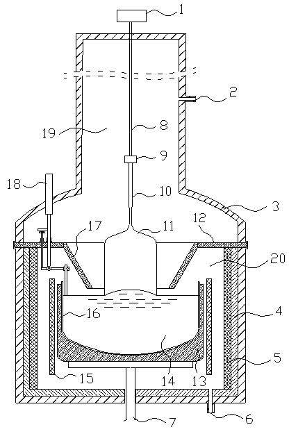
[0029] for the present invention figure 1 The shown single crystal furnace is combined with the auxiliary feeding structure described in the present invention to grow a high resistance N-type single crystal silicon ingot with low axial resistivity fluctuation.
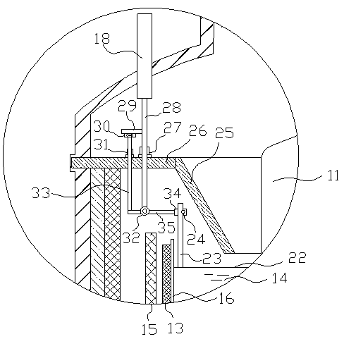
[0030] The Cz method is used to grow 8 inches of N-type single crystal silicon in the direction. Firstly, the coefficient of the load cell is calibrated by the standard weight, so that the weighing deviation is less than 3%. Subsequently, 120 kg of phosphorus-doped polysilicon raw material was put into the quartz crucible at one time. Process a p-type single crystal silicon rod of ϕ20×200mm, the average resistivity of the p-type single crystal silicon rod is 0.30Ω·cm, that is, the concentration of boron element inside the p-type single crystal silicon rod is about 3.7×10 13 atoms / cm 3 ; At the same time, process a groove at the position of 20mm from the end of the P-type monocrystalline silicon rod, and fix it on t...
Embodiment 2
[0034] for the present invention figure 1 The shown single crystal furnace is combined with the auxiliary feeding structure described in the present invention to grow N-type single crystal silicon ingots for power devices with ultra-low resistivity and low axial resistivity fluctuation.
[0035] The Cz method is used to grow an 8-inch N-type monocrystalline silicon ingot with direction, and the target resistivity value is 60-100Ω. Firstly, the weighing coefficient of the load cell 30 is calibrated by the standard weight, so that the weighing deviation is less than 3%. Subsequently, 120 Kg of boron-doped polysilicon raw materials were put into the quartz crucible at one time. Process a Si-Ga alloy rod of ϕ20×200mm, the mass ratio of Ga element in the alloy rod is 0.1%, and at the same time process a groove at the position of 20mm from the end of the Si-Ga alloy rod, after cleaning, use The latch is fixed on the accessory fixture 34 . Subsequently, close the main and auxilia...
Embodiment 3
[0039] for the present invention figure 1 The single crystal furnace shown in the present invention, in combination with the auxiliary feeding structure described in the present invention, grows a high-resistance P-type monocrystalline silicon ingot for power devices with low axial resistivity fluctuations. Generally, the resistivity is not lower than 50Ω.cm, and the resistivity The change rate requirement is preferably not higher than 15%.
[0040] The CZ method is used to grow 8-inch P-type single crystal silicon rods in the direction. Firstly, the coefficient of the load cell is calibrated by the standard weight, so that the weighing deviation is less than 3%. Subsequently, 120Kg of boron-doped polysilicon raw material was put into the quartz crucible at one time, and the initial concentration of boron was 1.78E14 atoms / cm 3 . Process a Si-P alloy rod with a size of ϕ20×200mm. The mass ratio of phosphorus in the alloy rod is 0.1%. A groove is processed at a position 20m...
PUM
| Property | Measurement | Unit |
|---|---|---|
| electrical resistivity | aaaaa | aaaaa |
| electrical resistivity | aaaaa | aaaaa |
| electrical resistivity | aaaaa | aaaaa |
Abstract
Description
Claims
Application Information

