Package-on-package structure of chip and package-on-package method

A stacked packaging and chip technology, applied in the direction of semiconductor/solid-state device components, semiconductor devices, electrical components, etc., can solve the problems of inconsistent tail wires, breakage and debonding, vibration fatigue, etc., and achieve the effect of reducing packaging resistance.

Active Publication Date: 2016-01-20
SILERGY SEMICON TECH (HANGZHOU) CO LTD
View PDF6 Cites 13 Cited by
  • Summary
  • Abstract
  • Description
  • Claims
  • Application Information

AI Technical Summary

Problems solved by technology

Excessive wire bonding of the prior art suffers from pad out pits, inconsis

Method used


Image

  • Package-on-package structure of chip and package-on-package method
  • Package-on-package structure of chip and package-on-package method
  • Package-on-package structure of chip and package-on-package method

Examples


no. 1 example

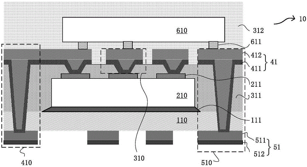
[0074] figure 1 It shows a schematic structural diagram of the stacked package structure of the first embodiment of the present invention. The package structure 10 mainly includes: a substrate 110, a first die 210, a first encapsulation body 311, a plurality of isolated interconnection bodies 310, a plurality of first redistribution bodies 410, a plurality of isolated penetrating bodies 510, The second die 610.

[0075] The substrate 110 may include semiconductor materials (such as silicon, germanium, indium antimonide, gallium arsenide, indium arsenide, gallium nitride, etc.), insulating materials (epoxy, polyester glass, silicon dioxide, polytetrafluoroethylene, etc.) Glass, ceramics, etc.) or a combination thereof. The packaging substrate 110 includes opposite first and second surfaces.

[0076] Both the first die 210 and the second die 610 include opposite active surfaces and back surfaces. The device layers of the first die 210 and the second die 610 are located on the acti...

no. 2 example

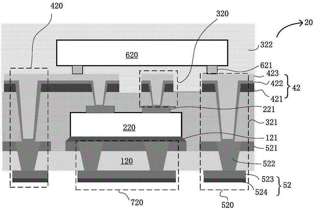
[0088] figure 2 The structure diagram of the stacked package structure of the second embodiment of the present invention is shown. The stacked package structure 20 includes: a substrate 120, a first die 220, a first encapsulation body 321, a plurality of isolated interconnections 320, a second encapsulation body 322, and a plurality of isolated first redistribution bodies 420, a plurality of isolated through bodies 520, a second die 620, a patterned conductive layer 521, and at least one second redistribution body 720.

[0089] The difference between this embodiment and the first embodiment is that the stacked package structure 20 further includes a conductive layer 521 and a second redistribution body 720. The patterned conductive layer 521 is formed on the first surface of the substrate 120, and the back surface of the first die 220 is electrically connected to the conductive layer 521 through the conductive adhesive layer 121, thereby leading the back electrode of the first d...

no. 3 example

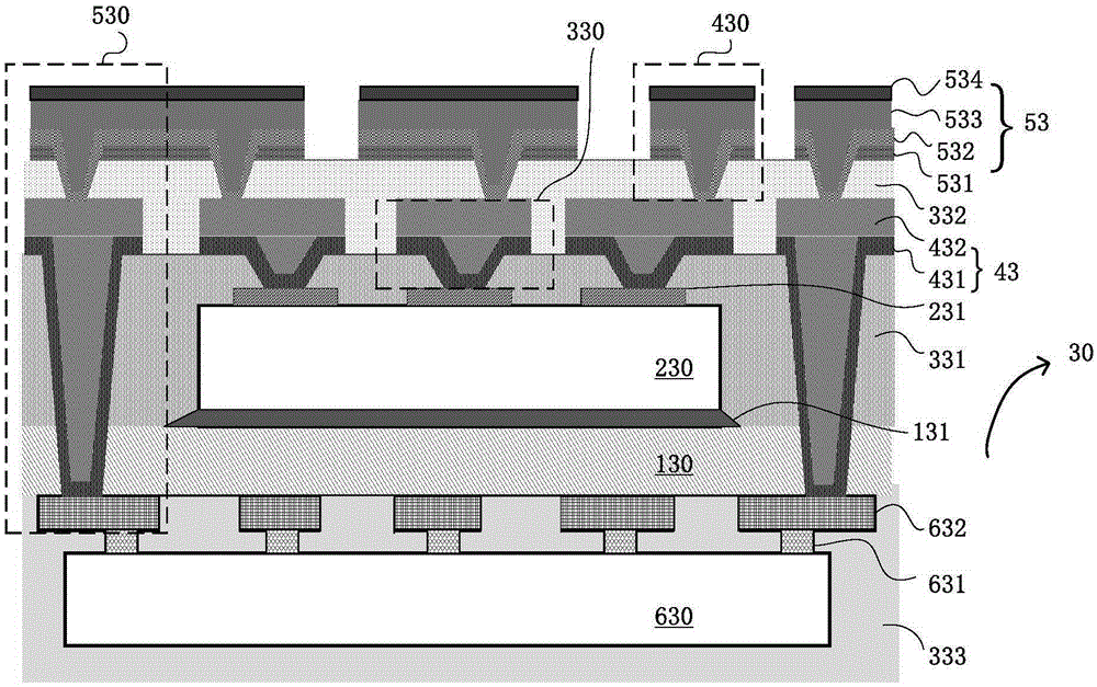
[0099] image 3 The structure diagram of the stacked package structure of the third embodiment of the present invention is shown. The stacked package structure 30 includes: a package substrate 130, a first die 230, an adhesive layer 131, a plurality of isolated interconnections 330, a first encapsulation body 331, and a plurality of isolated first redistribution bodies 430 , A plurality of isolated penetrating bodies 530, a second encapsulating body 322, a second die 630, and a third encapsulating body 333.

[0100] The back surface of the first die 230 is mounted on the first surface of the substrate 130 through the adhesive layer 131, and the substrate 130 also has a second surface opposite to the first surface. The first encapsulation body 331 covers the first die 230. The interconnection body 330 includes a first portion extending from the surface of the first encapsulation body 331 and a second portion extending from the surface of the first encapsulation body 331 to the p...


PUM


Abstract

The invention provides a package-on-package structure of a chip and a package-on-package method. In the package-on-package structure, an electrode is leaded out through an interconnector and a first rewiring member in packaging a first layer of pipe cores. The package-on-package structure and the package-on-package method are suitable for packaging the chip with relatively high pad spacing. Furthermore no bonding lead is required and a packaging resistance is reduced. Furthermore a penetrating member which penetrates a first packaging member and a substrate is used for leading the electrode on a second layer of the chip out, thereby realizing chip packaging in a package-on-package manner, effectively reducing the packaging area of an integrated circuit and number of pins.

Description

Technical field [0001] The invention relates to the technical field of chip packaging, in particular to a stacked packaging structure and a stacked packaging method of a chip. Background technique [0002] When manufacturing integrated circuits, the chips are usually packaged before integration with other electronic assemblies. This package usually includes sealing the chip in a material and providing electrical contacts on the outside of the package to provide an interface to the chip. Chip packaging can provide electrical connections from the chip to the motherboard of an electrical or electronic product, protection against pollutants, provide mechanical support, heat dissipation, and reduce thermomechanical strain. [0003] The connection between the internal chip and external pins of the semiconductor package plays an important role in establishing the input / output between the chip and the outside world, and is a key step in the packaging process. In order to reduce the area ...

Claims


Application Information

Patent Timeline
IPC IPC(8): H01L25/065H01L23/31H01L23/48H01L21/98
CPCH01L21/486H01L23/49827H01L25/0657H01L2224/02381H01L2224/02331H01L2224/0231H01L23/3121H01L25/03H01L25/50H01L2224/16225H01L2224/04105H01L2224/12105H01L2224/32225H01L2224/73267H01L2224/92244H01L24/19H01L2224/16227H01L2225/06527H01L2225/06572
Inventor 谭小春
Owner SILERGY SEMICON TECH (HANGZHOU) CO LTD
Why Eureka
Try Eureka