Sapphire composite substrate and preparing method thereof

A composite substrate, sapphire technology, applied in electrical components, circuits, semiconductor devices, etc., can solve the problems of low light extraction efficiency of light-emitting diodes, and achieve the effects of improved light extraction efficiency, improved brightness, and low cost

Inactive Publication Date: 2016-01-20
SHANDONG NOVOSHINE OPTOELECTRONICS CO LTD
View PDF5 Cites 11 Cited by
  • Summary
  • Abstract
  • Description
  • Claims
  • Application Information

AI Technical Summary

Problems solved by technology

However, the current sapphire substrate has low light extraction efficiency for light-emitting diodes due to its structural limitations.

Method used


Image

  • Sapphire composite substrate and preparing method thereof
  • Sapphire composite substrate and preparing method thereof
  • Sapphire composite substrate and preparing method thereof

Examples


Embodiment 1

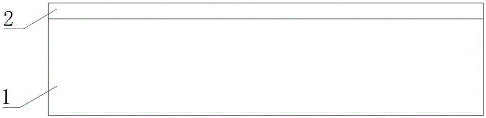
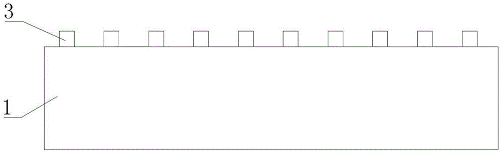
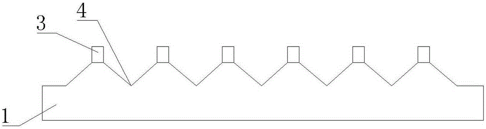
[0033] like figure 1 , figure 2 , image 3 , Figure 4 and Figure 5 As shown, a sapphire composite substrate includes a sapphire substrate 1, and a mask layer 2 is arranged on the sapphire substrate 1. The mask layer 2 forms a pattern mask layer 3 through photolithography or corrosion, and the pattern mask layer 3 protects and corrodes the sapphire. A patterned sapphire pattern layer 4 is formed on the substrate 1, and an aluminum oxide layer 5 is arranged on the patterned sapphire pattern layer 4. The thickness of the aluminum oxide layer 5 is 10-14nm or 101-500nm; the bottom of the adjacent pattern on the patterned sapphire pattern layer 4 Adhere to each other, the thickness of the mask layer is 10-5000nm, the mask layer is SiO2 mask layer 2, and the graphics on the SiO2 mask layer 2 are arranged in square or hexagonal arrangement.

[0034] The preparation method of the sapphire composite substrate of the present embodiment is a wet etching example, comprising steps: ...

Embodiment 2

[0044] This embodiment is basically the same as Embodiment 1, the difference is:

[0045] The preparation method is an example of dry etching, including steps:

[0046] 1. Choose a sapphire flat piece

[0047] 2. Using SiH4 / N2 mixed gas containing 5% SiH4 and N2O gas to deposit a SiO2 mask layer 2 with a thickness of 10-5000 nm on the sapphire flat sheet by plasma-enhanced vapor-phase chemical deposition.

[0048]3. Coating a layer of photoresist on the SiO2 mask layer 2, using photolithography technology to perform photoetching on the areas without patterns, so that the areas with patterns are protected by the photoresist to form the pattern mask layer 3.

[0049] 4. Using RIE to etch the SiO2 mask layer 2 with CF4 gas to obtain a pattern mask layer 3 with patterns arranged in a square or hexagonal arrangement.

[0050] 5. Continue to etch the sapphire to the bottom of the sapphire pattern by using BCl3, Cl3, H2, Ar, etc. by dry ICP, so that the bottoms of adjacent patterns...


PUM

PropertyMeasurementUnit
thicknessaaaaaaaaaa
thicknessaaaaaaaaaa

Abstract

The invention discloses a sapphire composite substrate and a preparing method thereof. The sapphire composite substrate comprises an alumina layer. The preparing method comprises the steps of growing a mask layer on a sapphire substrate which is cleaned to tidy, plating photoresist on the mask layer, then performing photoetching on the area without patterns on the mask layer by means of photoetching technology, etching by means of BOE solution or performing reactive ion etching (RIE) after photoetching, eliminating the mask layer area which is not protected by the photoresist, eliminating the residual photoresist by means of wet-method solution, etching the sapphire substrate under protection of the mask layer until the bottoms of adjacent patterns are connected, cleaning the patterned sapphire substrate according to a wet method, and depositing an aluminium nitride layer on the sapphire substrate by means of sputtering equipment, thereby forming the sapphire composite substrate. Therefore the preparing method of the sapphire composite substrate according to the invention can realize preparation of the large-area and low-cost industrialized composite patterned sapphire substrate.

Description

technical field [0001] The invention belongs to the technical field of micro-nano electronics manufacturing, relates to semiconductor materials, and in particular to a preparation method of a sapphire composite substrate. Background technique [0002] With the recent improvement of LED heat dissipation technology, LED high-power lighting fixtures such as high-power LED street lights and flood lights for outdoor lighting have been industrialized and have begun to be widely used. Stage lights and studio lights for indoor lighting that require high color temperature and color rendering have also been mass-produced and put into use. T8, T5, T4, lamp tubes for general lighting with the largest scope of application and the largest amount of consumption, and screw bulb lamps that replace incandescent lamps and energy-saving lamps have been serialized, and their service life has reached 50,000 hours. LED lighting has entered a period of rapid development. [0003] Usually, the gal...

Claims


Application Information

Patent Timeline
Patent Type & Authority Applications(China)
IPC IPC(8): H01L33/12H01L33/22H01L33/00
CPCH01L33/12H01L33/0066H01L33/22
Inventor 许南发王瑞敏玄成帅郭明灿
Owner SHANDONG NOVOSHINE OPTOELECTRONICS CO LTD
Why Eureka
Try Eureka