
Diamond substrate based nitride structure, preparation method and semiconductor device

A technology of diamond and nitride, which is applied in the field of semiconductor devices, can solve the problems of large nitride epitaxial layer mismatch, large thermal resistance at the interface of the diamond substrate, complex process, etc., to achieve good crystal quality, reduce lattice mismatch, Effect of reducing thermal resistance

Active Publication Date: 2016-02-10
DYNAX SEMICON
View PDF4 Cites 1 Cited by
  • Summary
  • Abstract
  • Description
  • Claims
  • Application Information

AI Technical Summary

Problems solved by technology

[0006] In view of this, the present invention proposes a nitride structure, preparation method and semiconductor device based on a diamond substrate to solve the problem of large mismatch between the nitride epitaxial layer grown on the diamond substrate and the interface between the nitride epitaxial layer and the diamond substrate. The problem of large thermal resistance and complex process

Method used


Image

  • Diamond substrate based nitride structure, preparation method and semiconductor device
  • Diamond substrate based nitride structure, preparation method and semiconductor device
  • Diamond substrate based nitride structure, preparation method and semiconductor device

Examples


Embodiment 1

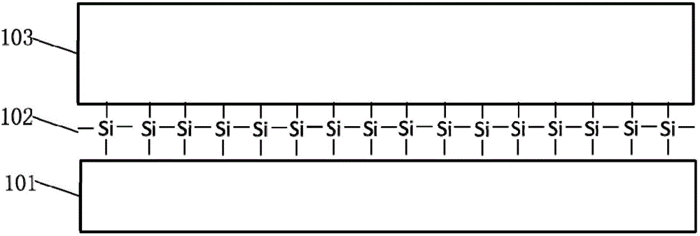
[0044] figure 1 is a schematic cross-sectional view of the nitride structure provided in Embodiment 1 of the present invention. Such as figure 1 As shown, the structure includes a diamond substrate 101 ; at least one group IV atomic layer 102 on the diamond substrate 101 ; and a nitride epitaxial layer 103 on the at least one group IV atomic layer 102 .

[0045] The above-mentioned diamond substrate 101 is relatively thick, which is different from the diamond prepared by MOCVD method on nitride, and it is not easy to warp, and will not cause excessive warping of the epitaxial wafer, so it is not necessary to use polishing and other means to solve the problem of the diamond substrate 101. The problem of warping is simple, and the thermal resistance of diamond is small, and the thermal conductivity is good. The specific thickness of the diamond substrate 101 can be adjusted according to the design requirements of the nitride structure.

[0046] In addition, the group IV atoms...

Embodiment 2

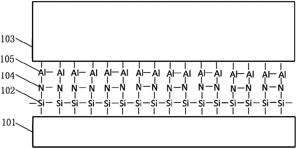
[0055] figure 2 It is a schematic cross-sectional view of the nitride structure provided by Embodiment 2 of the present invention. This embodiment is optimized on the basis of the above-mentioned embodiments, and the difference from Embodiment 1 is that there are sequentially stacked group V atomic layers 104 and III group atomic layer 105. Such as figure 2 As shown, the structure includes a diamond substrate 101; at least one IV group atomic layer 102 on the diamond substrate 101; a V group atomic layer 104 on the at least one IV group atomic layer 102; Group III atomic layer 105 above, and nitride layer 103 above group III atomic layer 105 .

[0056] Likewise, the aforementioned group IV atom may be a silicon atom. The atoms in the group V atomic layer 104 may be N, and the atoms in the group III atomic layer 105 may be Al. The group V atomic layer 104 and the group III atomic layer 105 can more smoothly transition the diamond substrate 101 from at least one group IV ...

Embodiment 3

[0069] image 3 It is a schematic cross-sectional view of the nitride structure provided by Embodiment 3 of the present invention. This embodiment is optimized based on the first embodiment, and the difference from the first embodiment is that the nitride epitaxial layer 103 includes a nucleation layer 106 located on at least one group IV atomic layer 102 . Such as image 3 As shown, the structure includes a diamond substrate 101 ; at least one group IV atomic layer 102 on the diamond substrate 101 ; and a nucleation layer 106 on the at least one group IV atomic layer 102 . The group IV atoms in this embodiment may be Si, and the material of the nucleation layer 106 may be AlN, GaN or AlGaN. The nucleation layer 106 can transition at least one group IV atomic layer 102 to the nitride epitaxial layer 103 to improve the crystal quality of the nitride epitaxial layer 103 .

[0070] The preparation method of the nitride structure of the present embodiment is as follows:

[007...


PUM


Abstract

The invention discloses a diamond substrate based nitride structure, a preparation method and a semiconductor device. The nitride structure comprises the diamond substrate, at least one layer of IV group atomic layer positioned on the diamond substrate, and a nitride epitaxial layer positioned on the at least one layer of the IV group atomic layer. According to the diamond substrate based nitride structure, the preparation method and the semiconductor device, the problems of high mismatch when the nitride epitaxial layer is growing on the diamond substrate, the high thermal resistance in the interface of the nitride epitaxial layer and the diamond substrate, and the complex technology are solved.

Description

technical field [0001] The invention relates to the technical field of semiconductors, in particular to a nitride structure based on a diamond substrate, a preparation method and a semiconductor device. Background technique [0002] As a power amplifier, GaN high electron mobility transistor (High Electron Mobility Transistor, HEMT) can be used in the fields of high-frequency and high-power devices such as radar systems, mobile communication systems and aerospace, and it also has great potential in the field of power electronic devices. Broad application prospects. However, the performance and reliability of current GaN microwave communication systems are limited by the high operating temperature caused by self-heating effects. Therefore, efficient thermal management is very important to reduce device heating and working area temperature. The use of large-volume metal heat sinks in GaNHEMT systems can provide a background with high thermal conductivity and reduce the tempe...

Claims


Application Information

Patent Timeline
Patent Type & Authority Applications(China)
IPC IPC(8): H01L29/778H01L29/06H01L29/20H01L21/335
CPCH01L29/0684H01L29/2003H01L29/66462H01L29/778
Inventor 张乃千吴传佳裴轶
Owner DYNAX SEMICON
Learn More