

Anti-reflection film, optoelectronic device, and manufacturing method for optoelectronic device
A technology of optoelectronic devices and anti-reflection coatings, applied in photovoltaic power generation, electrical components, semiconductor devices, etc., can solve the problems of narrow anti-reflection band, surface non-radiative recombination, and difficult preparation, so as to avoid reflection, improve efficiency, and manufacture The effect of simple process
- Summary
- Abstract
- Description
- Claims
- Application Information
AI Technical Summary
Problems solved by technology
Method used
Image

Examples
Embodiment 1
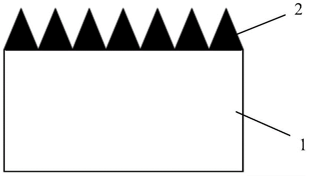
[0036] ginseng Figure 1a As shown, the optoelectronic device includes a semiconductor base layer 1 and a surface passivation antireflection layer 2 formed on the semiconductor base layer 1 .
[0037]The semiconductor base layer 1 can be a complete solar cell or a photoelectric conversion layer of a detector. For thin-film Si-based solar cells and other thin-film batteries, it includes the entire PN junction, that is, semiconductor materials such as the emitter layer and the base layer; for III-V batteries, this part includes the complete PN junction of each junction cell and the intermediate tunnel. The piercing junction also includes the window layer on the top layer, in short, this part includes all semiconductor layers used to absorb light.
[0038] The preparation method of the semiconductor base layer 1: for Si-based thin-film batteries, PECVD (plasma enhanced chemical vapor deposition method) is generally used; for organic batteries, spin-coating method is used; for CuI...
Embodiment 2
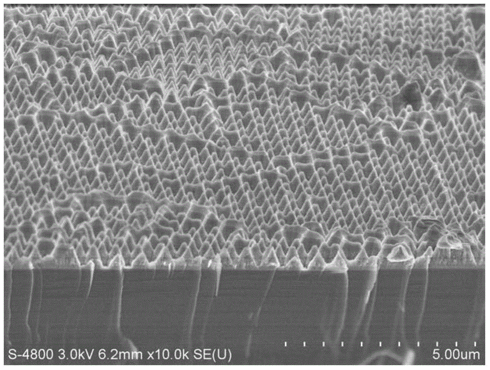
[0047] Figure 4 and Figure 5 The reflectance curves of SiN deposited on the surface of GaAs and the formation of micro-nano structures are given respectively ( Figure 4 ) and comparative analysis results of diffraction angle and critical angle under various periods ( Figure 5 ), the results also prove that adjusting the dielectric film and its micro-nano structure on the surface of III-V semiconductors can effectively reduce the incidence of III-V semiconductors when the high-order diffraction angle of the incident light is satisfied and the high-order diffraction angle is less than the critical angle of total reflection. surface reflection.
Embodiment 3
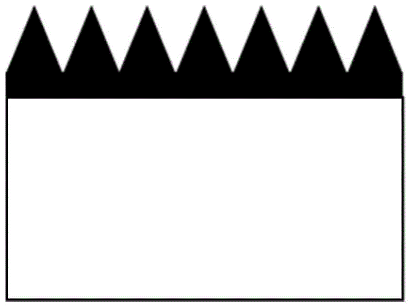
[0049] ginseng Image 6 As shown, the optoelectronic device includes a semiconductor base layer 10 and an antireflection layer 20 formed on the semiconductor base layer 10 .
[0050] The semiconductor base layer 10 may be a complete solar cell or a photoelectric conversion layer of a detector. For thin-film Si-based solar cells and other thin-film batteries, it includes the entire PN junction, that is, semiconductor materials such as the emitter layer and the base layer; for III-V batteries, this part includes the complete PN junction of each junction cell and the intermediate tunnel. The piercing junction also includes the window layer on the top layer, in short, this part includes all semiconductor layers used to absorb light.
[0051] The preparation method of the semiconductor base layer 10: for Si-based thin-film batteries, it is generally prepared by PECVD (Plasma Enhanced Chemical Vapor Deposition); for organic batteries, the spin coating method is used; for CuInGaSe, ...
PUM
 Abstract
Description
Claims
Application Information