Integrated stack double-junction perovskite solar cell and preparation method thereof

A solar cell and perovskite technology, which is applied in semiconductor/solid-state device manufacturing, circuits, photovoltaic power generation, etc. Through the effect of large loss, ultra-low energy consumption, and simple process equipment

Inactive Publication Date: 2016-02-17
XIANGTAN UNIV
View PDF6 Cites 26 Cited by
  • Summary
  • Abstract
  • Description
  • Claims
  • Application Information

AI Technical Summary

Problems solved by technology

However, the preparation process of CIGS solar cells has disadvantages such as relatively complicated, long preparation period, and indium being a rare metal. The manufacturing process of monocrystalline si

Method used


Image

  • Integrated stack double-junction perovskite solar cell and preparation method thereof

Examples


Embodiment 1

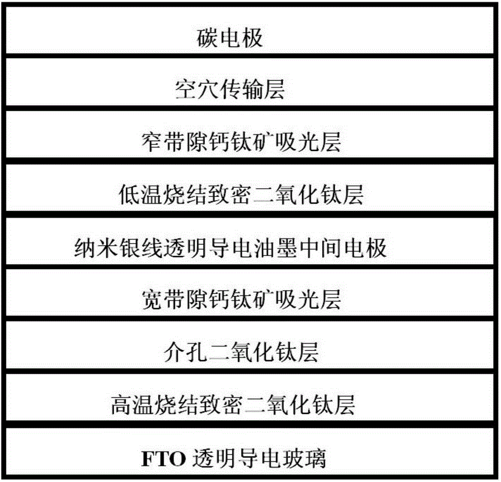
[0026] (1) Cleaning FTO transparent conductive glass: FTO transparent conductive glass is ultrasonically cleaned with deionized water, acetone, and ethanol for 15 minutes, dried with nitrogen, and then treated with a UV ozone cleaner to remove residual organic matter;

[0027] (2) Preparation of titanium dioxide dense layer: use spray pyrolysis to deposit a titanium dioxide dense layer on cleaned FTO transparent conductive glass, and annealed at 500°C for 60 minutes to obtain a titanium dioxide dense layer with a thickness of 50nm;

[0028] (3) Preparation of wide band gap perovskite light-absorbing layer: preheated CsSnI with a mass percentage concentration of 40% at 75°C in a glove box 3 The solution (using dimethylformamide as the solvent) was spin-coated on the titanium dioxide mesoporous layer preheated at 120°C at a speed of 2500 rpm. During the spin-coating period, hot air was blown to the surface of the titanium dioxide mesoporous layer to obtain a thickness of 500 nm. The n...

Embodiment 2

[0035] (1) Cleaning transparent conductive FTO glass: FTO glass is ultrasonically cleaned with deionized water, acetone, and ethanol for 15 minutes in sequence, dried with nitrogen, and then treated with an ultraviolet ozone cleaner to remove residual organic matter;

[0036] (2) Preparation of titanium dioxide dense layer: use spray pyrolysis to deposit a titanium dioxide dense layer on cleaned FTO conductive glass, and anneal it at 500°C for 60 minutes to obtain a titanium dioxide dense layer with a thickness of 50 nm;

[0037] (3) Preparation of wide band gap perovskite light-absorbing layer: preheated CsSnI with a mass percentage concentration of 40% at 75°C in a glove box 3 The solution (using dimethylformamide as the solvent) was spin-coated on the titanium dioxide mesoporous layer preheated at 120°C at a speed of 2500 rpm. During the spin-coating period, hot air was blown to the surface of the titanium dioxide mesoporous layer to obtain a thickness of 500 nm. The narrow band ...


PUM

PropertyMeasurementUnit
Bandgap widthaaaaaaaaaa
Thicknessaaaaaaaaaa
Thicknessaaaaaaaaaa

Abstract

The invention discloses an integrated stack double-junction perovskite solar cell and a preparation method thereof. The integrated stack double-junction perovskite solar cell is characterized in that the integrated stack double-junction perovskite solar cell comprises FTO transparent conductive glass, a high temperature sintering compact titanium dioxide layer, a wide band-gap perovskite light absorption layer, a silver nanowire transparent conductive ink intermediate electrode, a low temperature sintering compact titanium dioxide layer, a narrow band-gap perovskite light absorption layer, a hole transmission layer and a carbon electrode which are arranged from the bottom to the top in turn. Two perovskite light absorption layers with different band gaps are adopted so that range of light absorption spectrum of the cell is widened, an all-solution method preparation technology, which has advantages of ultralow energy consumption, simple technology equipment, low cost and short preparation period, is adopted, and thus photoelectric conversion efficiency of the perovskite solar cell can be greatly enhanced.

Description

Technical field [0001] The invention belongs to the technical field of laminated solar cell preparation, and specifically relates to an integrally stacked double-junction perovskite solar cell and a preparation method thereof. Background technique [0002] Solar cells are one of the most effective technical solutions in various clean energy technologies. They are of great significance for solving energy and environmental problems in the process of human development. Since the perovskite solar cell first appeared in 2009 with a photoelectric conversion efficiency of 3.8%, its efficiency has continued to rise at an unprecedented rate in the following short five years. As of December 12, 2014, the highest efficiency of perovskite solar cells certified by the National Renewable Energy Laboratory in the United States reached 20.1%. Therefore, it can be said that the perovskite solar cell represents the most meaningful breakthrough in the field of photovoltaic technology since the 187...

Claims


Application Information

Patent Timeline
IPC IPC(8): H01L51/42H01L51/44H01L51/46H01L51/48
CPCH10K71/13H10K71/12H10K85/30H10K30/151H10K30/82H10K2102/00Y02E10/549Y02P70/50
Inventor 王金斌李小磊钟向丽张阳李勃超
Owner XIANGTAN UNIV
Why Eureka
Try Eureka