Absorption structure of infrared quantum well photoelectric detector

A technology of photodetectors and absorption structures, applied in circuits, electrical components, semiconductor devices, etc., to achieve the effects of superior coupling efficiency, enhanced size, and large and weak dispersion

Active Publication Date: 2016-02-24
NANJING UNIV
View PDF4 Cites 2 Cited by
  • Summary
  • Abstract
  • Description
  • Claims
  • Application Information

AI Technical Summary

Problems solved by technology

[0003] However, for the commonly used n-type gallium arsenide (GaAs) QWIP, due to the selection rule of quantum absorption, it can only absorb the electric field component (E z )

Method used


Image

  • Absorption structure of infrared quantum well photoelectric detector
  • Absorption structure of infrared quantum well photoelectric detector
  • Absorption structure of infrared quantum well photoelectric detector

Examples


Embodiment Construction

[0025] The embodiments of the present invention are described in detail below. This embodiment is implemented on the premise of the technical solution of the present invention, and detailed implementation methods and specific operating procedures are provided, but the protection scope of the present invention is not limited to the following implementation example.

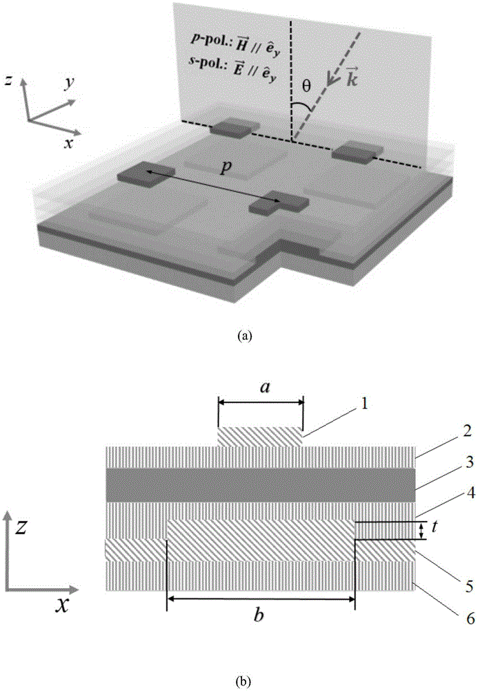
[0026] Such as figure 1 As shown, this embodiment is an optical coupling cavity with a metal (gold)-semiconductor-metal sandwich microstructure. The upper metal is a periodic gold square array 1 whose side length is defined as a, the lower layer is a gold plate 5 with a periodic gold square array, and the side length and thickness of the lower gold square are defined as b and t. The upper gold square array and the lower gold array have the same period (p) and symmetry. The multi-layer quantum well is placed in the middle of the metal layer, and the upper and lower contact layers 2 and 4 with a certain thickness a...


PUM


Abstract

The invention, which belongs to the field of the optical device in sub-wavelength photonics, discloses an absorption structure of an infrared quantum well photoelectric detector. The absorption structure for coupling incident electromagnetic waves to a quantum well active region comprises an upper metal layer, an intermediate semiconductor layer, and a lower metal layer. The upper metal layer is a periodic metal square array, the intermediate semiconductor layer is a quantum well layer, and the lower metal layer is a flat metal plate having a surface with the periodic metal square array. According to the absorption structure, on the basis of coupling of a micro-cavity mode excited by a metal microstructure and a hybridized SSPs mode, absorption of infrared radiation by the quantum well active region can be improved obviously and the electric field component (Ez) that is vital to quantum well absorption and is perpendicular to the quantum well plane is effectively enhanced, thereby overcoming a defect that the traditional quantum well infrared photoelectric detector does not absorb incident infrared radiation. With the structure, the detection efficiency of the ultra-far infrared photoelectric detector can be improved obviously.

Description

technical field [0001] The invention relates to the design of an absorption structure of an infrared quantum well photodetector, and belongs to the field of optical devices in subwavelength photonics. It specifically relates to an optical absorber structure with a metal-semiconductor-metal structure, which can efficiently localize infrared radiation and effectively enhance the electric field E z portion. Background technique [0002] Infrared detector is a kind of photoelectric conversion device with high sensitivity to infrared radiation, among which 14-16 micron very long wave infrared focal plane photodetector is the key technology of advanced weapon system and national defense modernization. According to the material system, infrared photodetectors can be divided into: the earliest developed mercury cadmium telluride (HgCdTe) system, and the quantum well infrared detector (QWIP) developed since the 1980s. It is well known that the infrared photoelectric conversion effi...

Claims


Application Information

Patent Timeline
Patent Type & Authority Applications(China)
IPC IPC(8): H01L31/101H01L31/0352
CPCH01L31/0352H01L31/035209H01L31/101
Inventor 王振林詹鹏刘垄陈聿
Owner NANJING UNIV
Why Eureka
Try Eureka