Superconducting fractal nanowire single-photon detector and preparation method thereof
A single-photon detector, nanowire technology, applied in superconductive devices, so-called superconductivity, superconductor components and other directions, can solve the problem of polarization sensitivity, achieve the effect of efficient absorption and reduce polarization sensitivity
- Summary
- Abstract
- Description
- Claims
- Application Information
AI Technical Summary
Problems solved by technology
Method used
Image
Examples
Embodiment 1
[0046] A superconducting fractal nanowire single photon detector. The overall technical scheme of the superconducting fractal nanowire single photon detector follows the following idea: first design a structure that reduces the low sensitivity of the nanowire to light absorption polarization, and then change the The arrangement of nano-antennas achieves high-efficiency absorption on the basis of low polarization sensitivity.
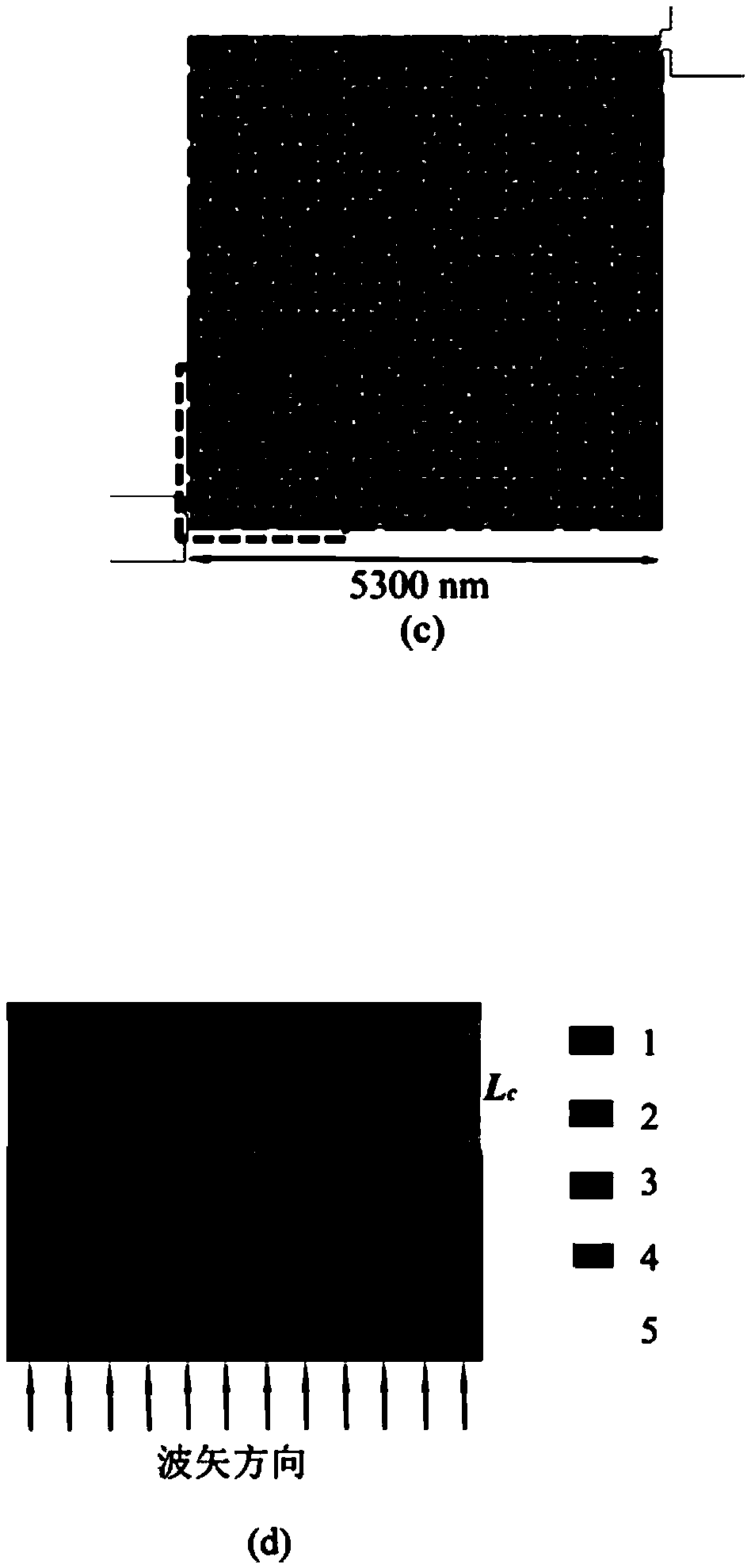
[0047] see figure 1 (d), the superconducting fractal nanowire single photon detector includes: substrate 1, nanowire 2, nanoantenna 3, hydrogen silsesquioxane layer 4 (HSQ) and silver reflective layer 5, nanowire 2 Arranged in a fractal form to ensure that the nanowires 2 are insensitive to the absorption polarization of light in two polarization states. A two-dimensional array nano-antenna 3 is added on the basis of the nano-wire 2 to increase light absorption efficiency.
[0048] The nanowire 2 in the embodiment of the present invention is composed o...
Embodiment 2
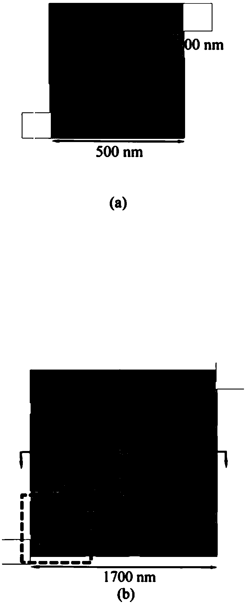
[0052] The following is combined with specific figure 1 (a), figure 1 (b) with figure 1 (c), and the corresponding mathematical formulas describe in detail the structure of the superconducting fractal nanowire single photon detector in Example 1, see below for details:
[0053] figure 1 (a) shows the structure of a fractal nanowire 2 (Peano structure). This type of nanowire 2 design is suitable for polycrystalline, monocrystalline or amorphous materials. figure 1 (b) with figure 1 The dashed box in (c) is the smallest structural unit that constitutes the secondary structure and the tertiary structure, and the black dashed line is the connection direction of the smallest structural unit. figure 1 (d) for figure 1 (b) The cross-sectional view cut by the solid black line in (b).
[0054] see figure 1 (d), the light is incident from bottom to top, L c is the length of the optical cavity; the electric field vibration direction of TM (transverse magnetic wave) is vertical t...
Embodiment 3
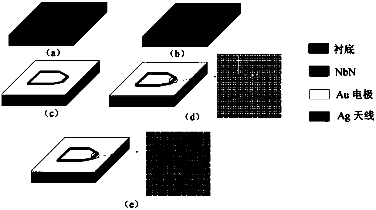
[0071] A kind of preparation method of superconducting fractal nanowire single photon detector, see figure 2 and image 3 , the preparation method comprises the following steps:
[0072] 101: sputtering a layer of superconducting material on the substrate 1 by means of magnetron sputtering;
[0073] 102: Prepare electrodes by combining photolithography and electron beam evaporation;
[0074] 103: Preparation of fractal nanowires 2 by combining electron beam exposure and reactive ion beam etching;
[0075] 104: Prepare the nano-antenna 3 by combining electron beam exposure (overlaying with the nanowire 2) and electron beam evaporation.
[0076] In summary, the embodiment of the present invention realizes the preparation of the superconducting fractal nanowire single photon detector through the above steps 101 to 104, which meets various needs in practical applications.
PUM
 Abstract
Description
Claims
Application Information


