Semiconductor device and method of manufacturing same
A semiconductor and device technology, applied in the field of semiconductor devices and their manufacturing, can solve problems such as the deterioration of transistor drive capability, achieve the effects of less characteristic deviation and improved performance
- Summary
- Abstract
- Description
- Claims
- Application Information
AI Technical Summary
Problems solved by technology
Method used
Image
Examples
no. 1 example
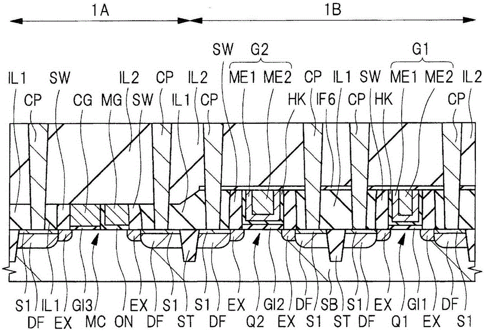
[0058] The semiconductor device according to the present embodiment and the following embodiments is equipped with a nonvolatile memory (nonvolatile memory element, flash memory, or nonvolatile semiconductor memory device). In this embodiment and the following embodiments, a description will be given of a nonvolatile memory by using a memory cell having an n-channel type MISFET (Metal Insulator Semiconductor Field Effect Transistor) as a base.
[0059] The polarity (the polarity of the voltage applied during the write / erase / read operation or the polarity of the carriers) in this embodiment and the next embodiment is used to describe MISFET operation in the case of memory cells. In the case of a memory cell having a p-channel MISFET as an underlying MISFET, in principle, the same operation can be achieved by reversing all polarities of applied potential, conductivity type of carriers, and the like. In the present application, the description will be made while distinguishing t...
no. 2 example
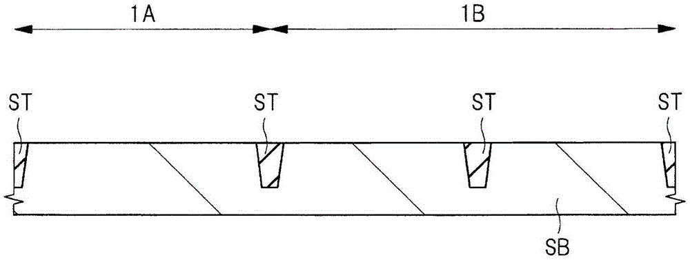
[0290] This embodiment and the above-mentioned reference Figure 1 to Figure 18 The described embodiments are different. In this embodiment, the gate electrode of the high breakdown voltage MISFET in the peripheral circuit area is composed of a silicide layer, and at this time the gate electrode has a control gate electrode and a memory gate electrode in the memory cell area equal to The height of each of them is lower than the height of the metal gate electrode constituting the low breakdown voltage MISFET in the peripheral circuit region. Figure 35 to Figure 39 are cross-sectional views of the semiconductor device of this embodiment during its respective manufacturing steps. and Figure 3 to Figure 18 resemblance, Figure 35 to Figure 39 A memory cell area 1A and a peripheral circuit area 1B are shown.
[0291] In the manufacturing steps of the semiconductor device of the present embodiment, firstly, performing and referring to Figure 3 to Figure 12 Similar steps to t...
PUM
| Property | Measurement | Unit |
|---|---|---|
| Specific resistance | aaaaa | aaaaa |
Abstract
Description
Claims
Application Information


