

Preparation method of large on-off ratio field effect transistor
A technology of field effect transistors and switching ratios, which is applied in the field of nano-electromechanical systems (NEMS), can solve the problems of unfavorable field-effect transistors widely used, achieve high response speed, ensure response speed, and overcome limitations
- Summary
- Abstract
- Description
- Claims
- Application Information
AI Technical Summary
Problems solved by technology
Method used
Image

Examples
Embodiment Construction
[0019] The present invention will be further described below in conjunction with the accompanying drawings and embodiments, but not as a basis for limiting the present invention.
[0020] Example. A preparation method of a field-effect transistor with a large switching ratio is characterized in that, the steps are as follows:
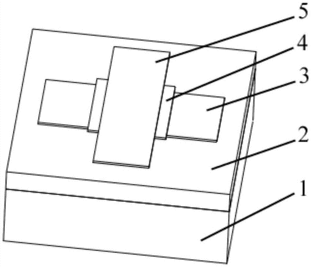
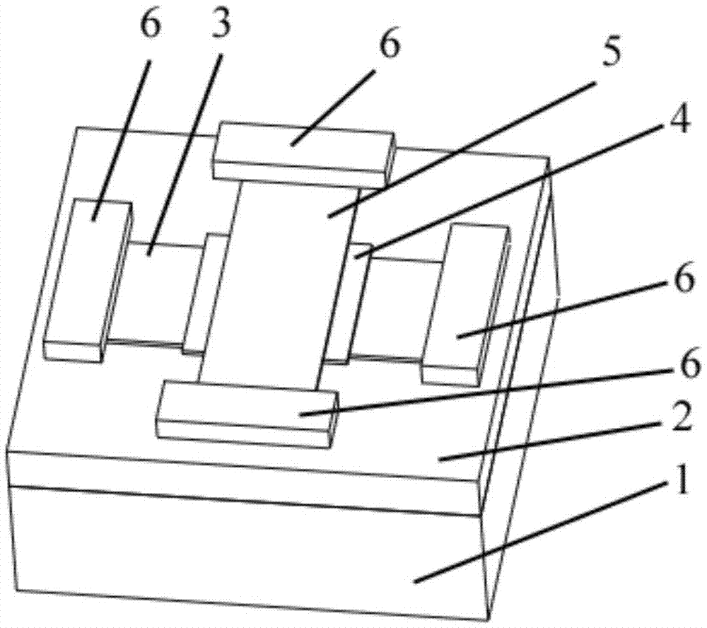
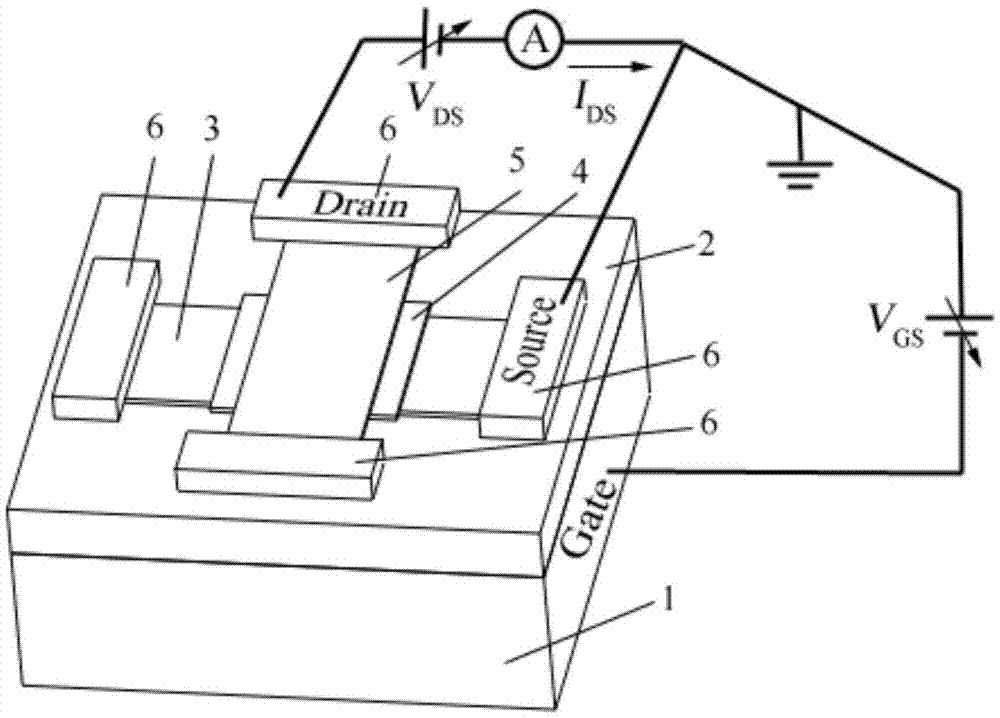
[0021] ① Prepare graphene flakes and tungsten disulfide flakes by mechanical exfoliation method, select single crystal silicon wafers with an oxide layer as the substrate, transfer graphene flakes, tungsten disulfide flakes, and graphene flakes to the substrate in sequence to form Graphene heterojunction;
[0022] ② Evenly spin-coat photoresist on the graphene heterojunction, then transfer the pattern on the mask plate to the photoresist through exposure, and use electron beam evaporation to deposit Ti / Au metal to obtain Ti / Au electrode, and obtain Graphene heterojunction based tunneling field effect transistor.
[0023] Preferably, the mec...
PUM
 Abstract
Description
Claims
Application Information