Lead welding device and technique for packaging semiconductor power device

A power device and lead wire welding technology, applied in the direction of tin feeding device, auxiliary device, welding medium, etc., can solve the problems of excessive diffusion depth, warpage, etc., and achieve small heat-affected area, high reliability, and high current resistance value Effect

Active Publication Date: 2016-04-06
王伟
View PDF5 Cites 4 Cited by
  • Summary
  • Abstract
  • Description
  • Claims
  • Application Information

AI Technical Summary

Problems solved by technology

If this point is ignored, many problems will be caused, such as warping caused by thermal stress, continuous diffusion caused by higher than the diffusion temperature, making the diffusion depth exceed the product setting value, etc.

Method used


Image

  • Lead welding device and technique for packaging semiconductor power device
  • Lead welding device and technique for packaging semiconductor power device
  • Lead welding device and technique for packaging semiconductor power device

Examples


Embodiment 1

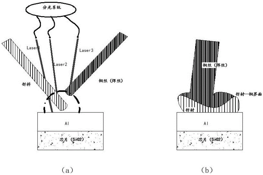
[0094] The present embodiment is the soldering welding of copper wire and chip aluminum pad, and copper wire and frame, and brazing material A is used for welding, and its chemical composition is (wt.%): Sn34.1%, Cu22.4%, Al20%, Ag2.0%, Bi3.5%, Sb9.0%, In9.0%.

[0095] The copper wire and the aluminum pad of the chip are welded to form the first solder joint, the preheating temperature is 220°C, the welding temperature is 290°C, the copper wire is welded to the copper frame to form the second solder joint, the preheating temperature is 220°C, and the welding temperature is 300°C.

Embodiment 2

[0099] The present embodiment is the soldering welding of copper wire and chip aluminum pad, and copper wire and frame, adopts solder A to carry out welding, and its chemical composition is (wt.%): Cu23.1%, Al18.7%, Ag3.5%, Bi3.5%, Sb8.3%, In8.0%, Sn balance.

[0100] The copper wire and the aluminum pad of the chip are welded to form the first solder joint, the preheating temperature is 220°C, the welding temperature is 290°C, the copper wire is welded to the copper frame to form the second solder joint, the preheating temperature is 220°C, and the welding temperature is 300°C.

Embodiment 3

[0104] This embodiment is the soldering welding of aluminum welding wire and chip aluminum pad, and aluminum welding wire and frame, adopts brazing material B to carry out welding, and its chemical composition is (wt.%): Sn34.1%, Cu21.0%, Al23.4%, Ag2.0%, Bi3.5%, Sb8.0%, In8.0%.

[0105] The aluminum wire is welded to the chip aluminum pad to form the first solder joint: the preheating temperature is 220°C, and the welding temperature is 290°C. The aluminum welding wire is welded with the copper frame to form the second solder joint: the preheating temperature is 220°C, and the welding temperature is 300°C.


PUM

PropertyMeasurementUnit
diameteraaaaaaaaaa
strengthaaaaaaaaaa
diameteraaaaaaaaaa

Abstract

The invention discloses a lead welding device and technique for packaging a semiconductor power device and belongs to the technical field of semiconductor power device packaging and manufacturing. The device is a laser wire welding machine and comprises a computer main board, a laser generator, a chip and frame image identification system, a feeding system and an XY workbench. The computer main board is used for controlling all the actions of the laser wire welding machine to achieve the whole automatic and accurate wire welding technique process; the laser generator is used for outputting laser spots of the required power and the required diameter; and the feeding system is used for accurately conveying a frame, a lead and a brazing wire to the work position before welding actions are executed. According to the technique, lead connection is achieved through a brazing technique, and the brazing process is achieved through lasers. By the adoption of the device and technique, a wet aluminum pad and a frame are directly melted to achieve the stable and reliable connection of the lead, a chip and the frame, and therefore mechanical damage, thermal damage and the stress problem existing in a traditional routing technique are avoided.

Description

technical field [0001] The invention relates to the technical field of semiconductor power device packaging and manufacturing, in particular to a wire welding device and process for semiconductor power device packaging. Background technique [0002] In nature, the electrical conductivity and thermal conductivity of copper are second only to silver, and the affinity between copper and humans is second only to titanium. Therefore, copper has been widely used in the fields of electricity transmission, heat exchange and daily necessities. Applications. [0003] In the packaging and manufacturing process of semiconductor power devices, considering the characteristics of high current, high calorific value and ultra-high power of power devices, it is decided to use copper instead of or partially replace aluminum wires to complete the connection between chips and pins, and the most critical link , that is to realize the stable connection between the copper wire (copper wire or stri...

Claims


Application Information

Patent Timeline
Patent Type & Authority Applications(China)
IPC IPC(8): B23K1/005B23K3/00B23K3/06B23K3/08B23K35/26B23K35/40
CPCB23K1/0056B23K3/00B23K3/063B23K3/08B23K35/262B23K35/40
Inventor 王伟
Owner 王伟
Why Eureka
Try Eureka