Method for constructing large-area, flexible, wearable organic nano-wire field-effect transistor array by using adhesive tape as substrate

A technology of field-effect transistors and nanowire arrays, applied in the field of organic nanowire field-effect transistor arrays, can solve problems such as limitations, less research, and difficult transfer processes, and achieve the effects of maintaining proper performance, low cost, and simple processes

Active Publication Date: 2016-04-06
SUZHOU UNIV
View PDF6 Cites 5 Cited by
  • Summary
  • Abstract
  • Description
  • Claims
  • Application Information

AI Technical Summary

Problems solved by technology

At the same time, the transfer of organic nanowire arrays to flexible devices has good bending resistance. However, through traditional microelectronics processing technology, photolithography on adhesive tape is difficult, and there are few studies. Most organic nanowire arrays are constructed on SiO2 / Si and glass substrates, and the choice of substrates is limited. Therefore, it is urgent to transfer organic nanowire arrays to scotch tape through a simple and effective method.

Method used


Image

  • Method for constructing large-area, flexible, wearable organic nano-wire field-effect transistor array by using adhesive tape as substrate
  • Method for constructing large-area, flexible, wearable organic nano-wire field-effect transistor array by using adhesive tape as substrate
  • Method for constructing large-area, flexible, wearable organic nano-wire field-effect transistor array by using adhesive tape as substrate

Examples


preparation example Construction

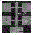
[0036] 4) Preparation of the insulating layer: use the magnetron sputtering method to coat a layer of Si3N4 on the plated gate substrate as the insulating layer;

[0037] 5) Preparation of source and drain electrodes: on the substrate coated with an insulating layer, metal material gold is deposited as source and drain electrodes by photolithography, development, and evaporation;

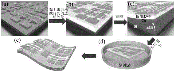
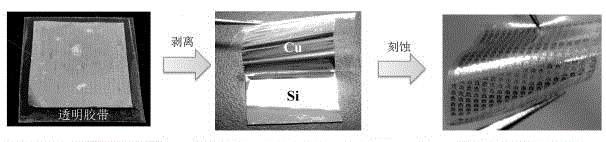
[0038] 6) Growth and transfer of nanowire arrays: With the assistance of gratings, PDMS templates are prepared, nanowire arrays are grown by physical vapor deposition (PVD), and nanowire arrays are transferred to the tape using tape, and then transferred to the plated electrodes on Cu / Si substrates.

[0039] 7) Device construction: Since the adhesive force between the adhesive tape and copper is stronger than that between silicon and copper, the adhesive force of the adhesive tape can be used to directly separate the copper from the silicon substrate, and further separate the electrodes and nanowire...


PUM

PropertyMeasurementUnit
thicknessaaaaaaaaaa
thicknessaaaaaaaaaa

Abstract

The invention relates to a method for constructing a large-area, flexible, wearable organic nano-wire field-effect transistor array by using an adhesive tape as a substrate. The method comprises: (1), carrying out nano wire growth; to be specific, preparing a template and growing a nano-wire array on the template in a self-assembling mode; (2), manufacturing a substrate; to be specific, carrying out sacrificial layer plating on sacrificial substrate surface and manufacturing a gate electrode, a source electrode, and drain electrode on the sacrificial layer; (3), carrying nano wire transferring; to be specific, laying an adhesive tape on the template with the grown nano-wire array to enable the nano-wire array to be attached to the transparent adhesive tape, stripping the adhesive tape, and transferring and attaching the adhesive tape with the attached nano-wire array to the substrate manufactured at the step (2); and constructing a device; to be specific, separating the sacrificial layer from the sacrificial substrate by using the characteristic that the adhesive power between the adhesive tape and the sacrificial layer is larger than the adhesive power between the sacrificial substrate and the sacrificial layer, and transferring the sacrificial layer into a sacrificial layer etching solution for etching, thereby obtaining a transistor array using the adhesive tape as the substrate.

Description

technical field [0001] The invention discloses a method for constructing a large-area, high-performance, flexible and wearable organic nanowire field-effect transistor array by using a scotch tape as a base and utilizing a tape stripping process. Specifically, the present invention relates to a process combining dry method and wet method transfer and etching, which realizes the preparation method of devices transferred from a silicon substrate to a flexible scotch tape substrate. Background technique [0002] As a daily necessities, scotch tape has the properties of being easy to bend, fold, and stick, and has great potential for applications in flexible electronic devices, such as biological devices, ultra-lightweight devices, wearable electronic devices, smart clothing, skin Sensing etc. Based on the consideration of flexibility and electronic device performance, one-dimensional large-area self-assembled organic single-crystal nanowire arrays have better flexibility than ...

Claims


Application Information

Patent Timeline
Patent Type & Authority Applications(China)
IPC IPC(8): H01L51/40
CPCH10K71/80
Inventor 揭建胜邓巍王亮
Owner SUZHOU UNIV
Why Eureka
Try Eureka