

Visible light bidirectional absorber structure
An absorber and visible light technology, which is applied in the direction of microstructure technology, microstructure devices, and manufacturing microstructure devices, etc., can solve the problem that visible light absorber junctions cannot achieve perfect absorption of bidirectional incident light at the same time, and the absorption efficiency of light absorbers is inherently limited. Solve problems such as waste of light energy, achieve the effect of bidirectional visible light absorption, simple structure, and low material consumption
- Summary
- Abstract
- Description
- Claims
- Application Information
AI Technical Summary
Problems solved by technology
Method used
Image

Examples
Embodiment 1
[0024] The manufacturing process of a visible light two-way absorber in this embodiment is as follows:
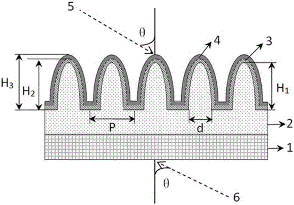
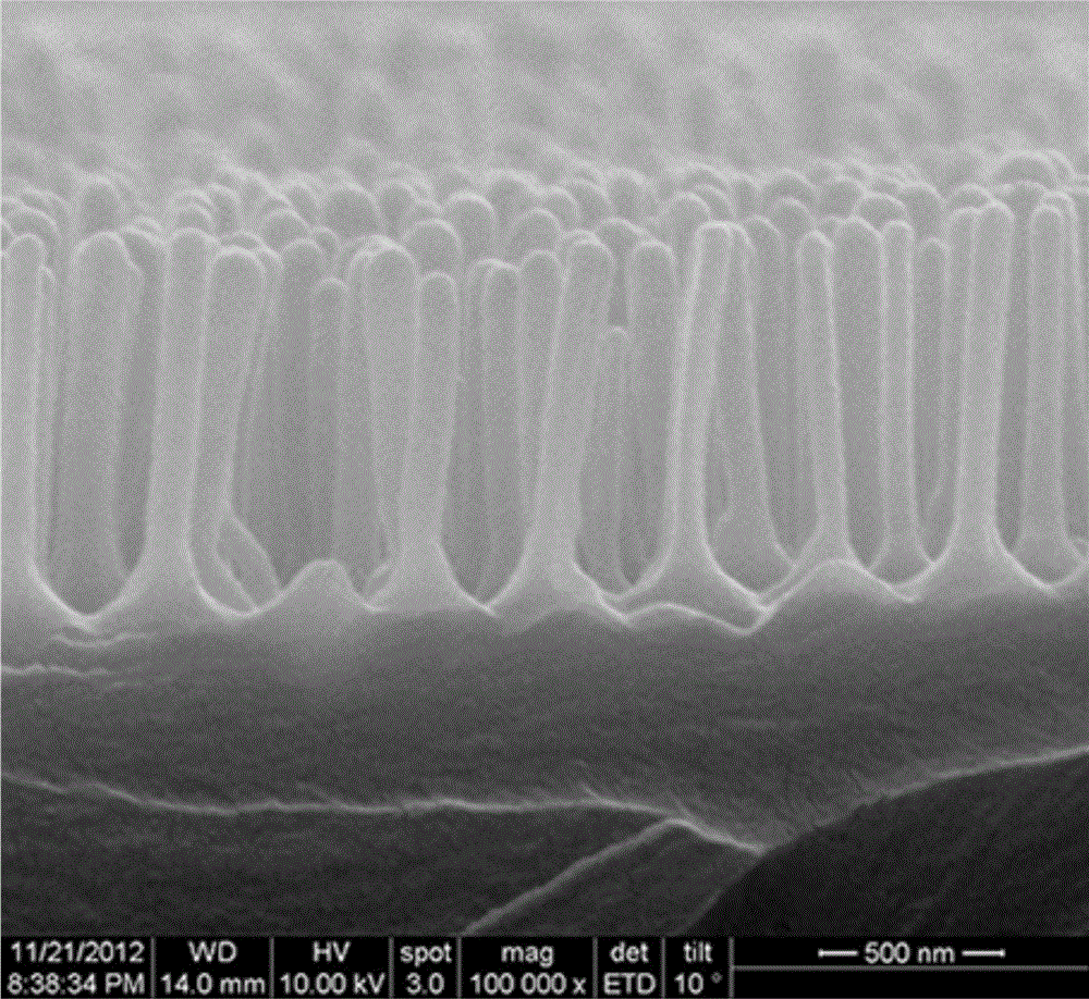
[0025] (1) Using polyethylene terephthalate as the substrate material, using the well-known technology in the field that we reported earlier - soft nanoimprint technology (Advanced Functional Materials, 25(18), 2660-2668), on the substrate The preparation material is the nanostructure unit of ultraviolet curable adhesive (such as figure 2 shown), the period of the nanostructure unit is P=180nm, and the height is H 1 =300nm, the bottom width is d=65nm;
[0026] (2) A layer of metal Au is evaporated on the above-mentioned nanostructure unit by thermal evaporation method, with a thickness (H 3 -H 2 )=20nm;
[0027] (3) Using the magnetron sputtering method to make a dielectric layer silicon nitride film (Si 3 N 4 ), thickness (H 3 -H 2 )=18nm.
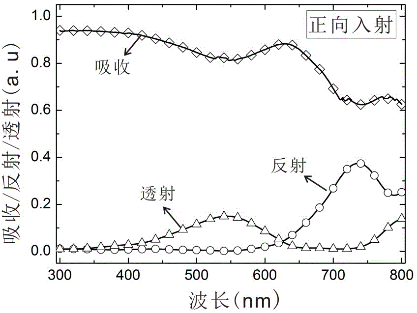
[0028] Ultimately, as Figure 3a As shown, the forward average absorption rate of the obtained visible two-way absorber de...
Embodiment 2
[0030] The manufacturing process of a visible light two-way absorber in this embodiment is as follows:
[0031] (1) The preparation of the nanostructure unit is the same as step (1) in Example 1;
[0032] (2) adopt measurement and control sputtering method to make a layer of metal Ni on the above-mentioned nanostructure unit, thickness (H 3 -H 2 )=15nm;
[0033] (3) adopt magnetron sputtering method to make medium layer silicon nitride film (Si 3 N 4 ) thickness (H 3 -H 2 )=10nm.
[0034] The result is as Image 6As shown, the obtained visible two-way absorber device has a forward average absorption rate of 89.1% in the entire 300nm-800nm visible light band, and a corresponding reverse average absorption rate of 67.4%.
Embodiment 3
[0036] The manufacturing process of a visible light two-way absorber in this embodiment is as follows:
[0037] (1) A single crystal silicon wafer is used as the base material, and the nanostructure unit is prepared on the single crystal silicon wafer by electron beam etching method, the period is P=120nm and the height is H 1 =250nm, the bottom width is d=60nm;
[0038] (2) A layer of metal Au is evaporated on the above-mentioned nanostructure unit by thermal evaporation method, with a thickness (H 3 -H 2 )=15nm;
[0039] (3) The dielectric layer silicon dioxide (SiO2) is made on the metal layer Au by thermal evaporation method. 2 ), thickness (H 3 -H 2 )=22nm.
[0040] Test the forward and reverse absorption rate of the prepared device, the results are as follows Figure 7 As shown, the obtained visible two-way absorber device has a forward average absorption rate of 88.1% in the entire 300nm-800nm visible light band, and a corresponding reverse average absorption r...
PUM
| Property | Measurement | Unit |
|---|---|---|
| thickness | aaaaa | aaaaa |
| height | aaaaa | aaaaa |
| width | aaaaa | aaaaa |
Abstract
Description
Claims
Application Information