Multielement metal oxide thin film based resistive random access memory and preparation method therefor

A technology of oxide film and multiple metals, applied in the field of memory, can solve the problems of high cost and low switching voltage, and achieve the effect of improving performance, low switching voltage, and stable anti-fatigue characteristics

Inactive Publication Date: 2016-04-27
UNIV OF ELECTRONIC SCI & TECH OF CHINA
View PDF2 Cites 4 Cited by
  • Summary
  • Abstract
  • Description
  • Claims
  • Application Information

AI Technical Summary

Problems solved by technology

[0005] The object of the present invention is to provide a resistive variable memory based on a multi-element metal oxide film and a preparation method thereof. The resistive variable memory of the present invention has a high switc

Method used


Image

  • Multielement metal oxide thin film based resistive random access memory and preparation method therefor
  • Multielement metal oxide thin film based resistive random access memory and preparation method therefor

Examples


Embodiment 1

[0023] 1. Clean the substrate: select polyimide (PI) as the substrate, scrub the substrate with alcohol to remove organic impurities, rinse the substrate with deionized water several times, and then dry it with ordinary nitrogen, repeat the above steps The steps are repeated until the substrate is clean and ready for use.

[0024] 2. Preparation of resistive memory based on CuGaZnO

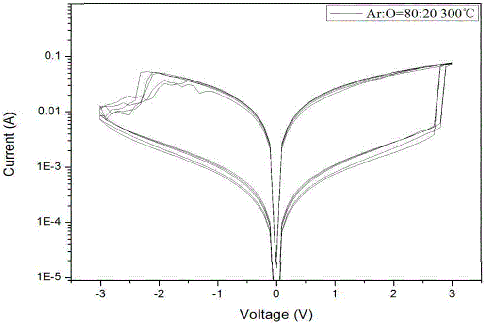
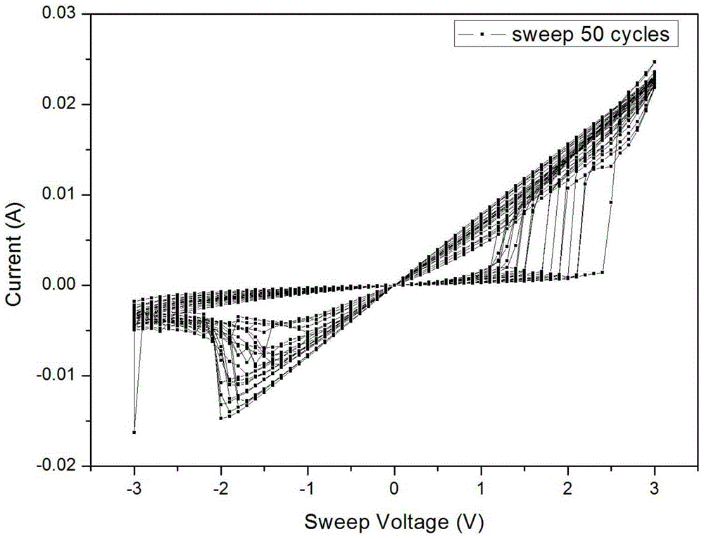
[0025] 1) Prepare the bottom electrode: in the chamber of the RF magnetron sputtering coating system, select ZnO doped with 2at% Al as the target material, install it on the target stage, and place the quartz substrate on the substrate stage; The chamber is evacuated to 3.3 x 10 -3 Pa, and then flow argon gas with a flow rate of 80 sccm, set the substrate temperature at 300° C., and sputter for 2 hours at a power of 50 W to form a bottom electrode.

[0026] 2) Preparation of the resistive switch layer: take out the prepared bottom electrode substrate, and paste a mask on one side of the substrat...

Embodiment 2

[0029] 1. Clean the substrate: select polyimide (PI) as the substrate, scrub the substrate with alcohol to remove organic impurities, rinse the substrate with deionized water several times, and then dry it with ordinary nitrogen, repeat the above steps The steps are repeated until the substrate is clean and ready for use.

[0030] 2. Preparation of resistive memory based on CuGaZnO

[0031] 1) Prepare the bottom electrode: in the chamber of the RF magnetron sputtering coating system, select ZnO doped with 2at% Al as the target material, install it on the target stage, and place the quartz substrate on the substrate stage; The chamber is evacuated to 3.3 x 10 -3 Pa, and then flow argon gas with a flow rate of 80 sccm, set the substrate temperature at 100° C., and sputter for 2 hours at a power of 50 W to form a bottom electrode.

[0032] 2) Preparation of the resistive switch layer: take out the prepared bottom electrode substrate, and paste a mask on one side of the substrat...

Embodiment 3

[0035] Clean the substrate: select polyimide (PI) as the substrate, scrub the substrate with alcohol to remove organic impurities, rinse the substrate with deionized water several times, and then dry it with ordinary nitrogen, repeat the above steps for more Repeat until the substrate is clean before use.

[0036] 2. Preparation of resistive memory based on CuGaZnO

[0037] 1) Prepare the bottom electrode: in the chamber of the RF magnetron sputtering coating system, select ZnO doped with 2at% Al as the target material, install it on the target stage, and place the quartz substrate on the substrate stage; The chamber is evacuated to 3.3 x 10 -3 Pa, and then flow argon gas with a flow rate of 80 sccm, set the substrate temperature at 200° C., and sputter for 2 hours at a power of 50 W to form a bottom electrode.

[0038] 2) Preparation of the resistive switch layer: take out the prepared bottom electrode substrate, and paste a mask on one side of the substrate with aluminum f...


PUM


Abstract

The invention discloses a multielement metal oxide thin film based resistive random access memory and a preparation method therefor, and belongs to the technical field of a memory. A bottom electrode layer, a resistive random layer and a top electrode layer are arranged on a substrate in sequence; the bottom electrode material is 2at% Al doped ZnO; the resistive random layer is CuGaZnO; and the top electrode material is Cu. The preparation method comprises the following steps of adopting a radio frequency magnetron sputtering method to prepare the bottom electrode on the substrate; placing a metal mask on the bottom electrode layer; then preparing the CuGaZnO thin film on the metal mask to form the resistive random layer; and finally adopting a vacuum coating technology to prepare the Cu top electrode on the CuGaZnO thin film so as to form the bottom electrode-resistive random layer-top electrode structure. The resistive random access memory has the characteristics of high switch ratio, relatively low switching voltage, stable retention, and anti-fatigue; the problem of high cost of the material of the resistive random layer in the preparation process is effectively solved; and the preparation process is high in portability, and the implementation of a full-transparent device can be facilitated.

Description

technical field [0001] The invention belongs to the technical field of storage devices, and in particular relates to a resistive storage device based on a multi-element metal oxide thin film and a preparation method thereof. Background technique [0002] In recent years, with the rapid development of semiconductor technology, the size of semiconductor memory is getting smaller and smaller, and the storage capacity is getting bigger and bigger. However, with the improvement of device integration, traditional Flash memory encounters more stringent physical limitations, so people have been looking for new non-volatile memory to replace traditional Flash memory. New types of non-volatile memories such as phase change memory, resistive change memory, ferroelectric memory and magnetic random access memory have attracted extensive research. Among them, resistive memory has become a research hotspot due to its advantages. [0003] An important component of a resistive memory (RRAM...

Claims


Application Information

Patent Timeline
IPC IPC(8): H01L45/00
CPCH10N70/20H10N70/883H10N70/026H10N70/826
Inventor 韦敏邓意峰邓宏
Owner UNIV OF ELECTRONIC SCI & TECH OF CHINA
Why Eureka
Try Eureka