Field emission cathode and preparation method and application thereof
A field emission cathode and molybdenum disulfide technology, which is applied in the field of field emission, can solve the problems of small emission current, application limitation, and poor emission stability, and achieve the effects of reducing contact resistance, reducing production cost, and stable performance
- Summary
- Abstract
- Description
- Claims
- Application Information
AI Technical Summary
Problems solved by technology
Method used
Image

Examples
preparation example Construction
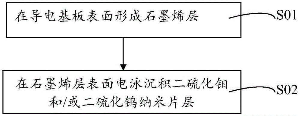
[0032] On the other hand, on the basis of the field emission cathode of the embodiment of the present invention described above, the embodiment of the present invention also provides a preparation method of the field emission cathode of the embodiment of the present invention. The preparation method of the field emission cathode of the embodiment of the present invention is as follows figure 2 Therefore, see also figure 1 , its preparation method comprises the following steps:
[0033] S01. Forming a graphene layer 2 on the surface of the conductive substrate 1;
[0034] S02. Electrophoretic deposition of molybdenum disulfide and / or tungsten disulfide nanosheet layer 3 on the surface of graphene layer 2:
[0035] Molybdenum disulfide and / or tungsten disulfide nanosheets and charge additives are dispersed in an organic solvent to form an electrophoretic solution, the conductive substrate is used as a negative electrode, and under the action of an external electric field, the m...
Embodiment 1
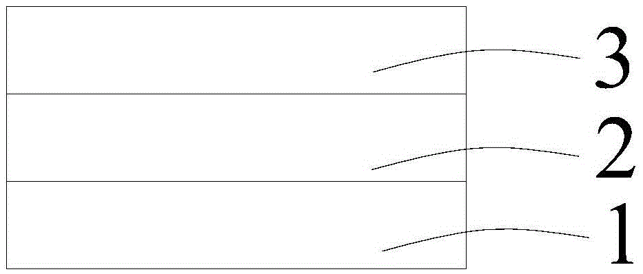
[0059] The embodiment of the present invention provides a field emission cathode and a preparation method thereof. Among them, the field emission cathode structure such as figure 1 As shown, it includes a conductive substrate 1 / graphene layer 2 / molybdenum disulfide nanosheet layer 3 sequentially stacked and combined. Wherein, the conductive substrate 1 material is a copper sheet; the thickness of the graphene layer 2 is 5nm; The thickness is 3-5 μm.
[0060] Its preparation method is as follows:
[0061] S11. Provide conductive substrate: copper sheet
[0062] S12. chemical vapor deposition (CVD) method growth graphene layer:
[0063] Put the conductive substrate coated with the catalyst metal layer into the reaction furnace, pass in argon (Ar), heat the substrate to the reaction temperature of 900 ° C, keep it warm for a period of time, and then pass in methane and hydrogen (H 2 ) mixed gas to grow graphene nanosheets for 5min. After the reaction was over, it was cooled ...
Embodiment 2
[0068] The embodiment of the present invention provides a field emission cathode and a preparation method thereof. Among them, the field emission cathode structure such as figure 1 As shown, it includes a conductive substrate 1 / graphene layer 2 / molybdenum disulfide nanosheet layer 3 sequentially stacked and combined. Among them, the material of conductive substrate 1 is n-type doped silicon sheet; the thickness of graphene layer 2 is 10nm; The thickness of the molybdenum nanosheet layer 3 is 8-10 μm.
[0069] Its preparation method is as follows:
[0070] S21. Provide conductive substrate: n-type doped silicon wafer
[0071] S22. chemical vapor deposition (CVD) method growth graphene layer:
[0072] Put the conductive substrate coated with the catalyst metal layer into the reaction furnace, pass in argon (Ar), heat the substrate to the reaction temperature of 900 ° C, keep it warm for a period of time, and then pass in methane and hydrogen (H 2 ) mixed gas to grow graphen...
PUM
| Property | Measurement | Unit |
|---|---|---|
| Thickness | aaaaa | aaaaa |
| Thickness | aaaaa | aaaaa |
| Horizontal size | aaaaa | aaaaa |
Abstract
Description
Claims
Application Information
 - R&D
- Intellectual Property
- Life Sciences
- Materials
- Tech Scout
- Unparalleled Data Quality
- Higher Quality Content
- 60% Fewer Hallucinations
Browse by: Latest US Patents, China's latest patents, Technical Efficacy Thesaurus, Application Domain, Technology Topic, Popular Technical Reports.
© 2025 PatSnap. All rights reserved.Legal|Privacy policy|Modern Slavery Act Transparency Statement|Sitemap|About US| Contact US: help@patsnap.com