Low-noise avalanche photodetector and preparation method thereof

A technology of avalanche optoelectronics and detectors, applied in circuits, electrical components, semiconductor devices, etc., can solve the problem of low working bandwidth

Active Publication Date: 2016-05-11
WUHAN IND INST FOR OPTOELECTRONICS
View PDF3 Cites 17 Cited by
  • Summary
  • Abstract
  • Description
  • Claims
  • Application Information

AI Technical Summary

Problems solved by technology

But at the same time, we noticed that the working bandwidth of avalanche photodetectors is much lower than that of ordinary photodetectors due to the limitation of avalanche establishment time

Method used


Image

  • Low-noise avalanche photodetector and preparation method thereof
  • Low-noise avalanche photodetector and preparation method thereof
  • Low-noise avalanche photodetector and preparation method thereof

Examples


Embodiment 1

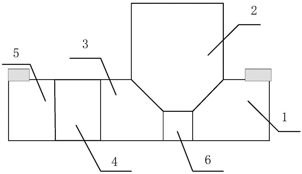
[0022] As embodiment 1, the present invention discloses a Si / Ge avalanche photodetector, its structure is as attached figure 1 shown. The structure of this detector includes but is not limited to: P-type ohmic contact layer 1, absorption layer 2, charge layer 3, multiplication layer 4, heavily doped N-type ohmic contact layer 5 and Si substrate 6, wherein the specific structural parameters As shown in Table 1.

[0023]

[0024]

[0025] Table 1

[0026] The present invention is characterized in that the one-dimensional avalanche photodetector is improved into a two-dimensional structure, and the k value is reduced by using the dead zone effect. The N-type and P-type ohmic contact layers are formed by high doping at both lateral ends of the low-doped silicon layer, and the doping concentration is higher than 1.0×10 18 / cm 3 . The charge layer is formed between the P-type and N-type ohmic contact layers using precisely controlled P-type or N-type doping, and the dopin...

Embodiment 2

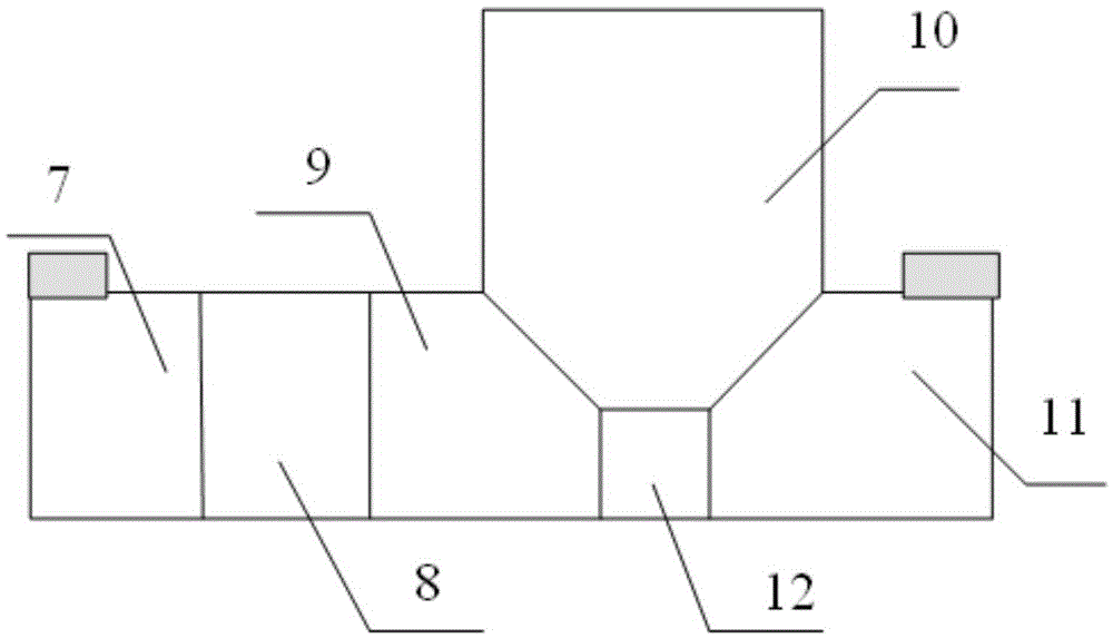
[0033] As embodiment 2, the present invention discloses an InP / InGaAs avalanche photodetector, the structure of which is shown in the attached image 3 . The structure of this detector includes but is not limited to: P-type ohmic contact layer 7, multiplication layer 8, charge layer 9, absorption layer 10, heavily doped N-type ohmic contact layer 11 and InP substrate 12, wherein the specific structural parameters As shown in table 2.

[0034]

[0035] Table 2

[0036] Embodiment 2 provides a method for manufacturing the above-mentioned InP / InGaAs avalanche photodetector, including the following steps:

[0037] S1. Make regions of different doped InP materials, and sequentially form P-type ohmic contact layer 7, multiplication layer 8, charge layer 9, and heavily doped N-type ohmic contact layer on InP by diffusion, ion implantation and other processes. 11; and an InP substrate 12 is formed at the bottom between the charge layer 9 and the heavily doped N-type ohmic contac...


PUM


Abstract

The invention discloses a low-noise avalanche photodetector and a preparation method thereof. The low-noise avalanche photodetector comprises an N-type ohmic contact layer/P-type ohmic contact layer, a multiplication layer, a charge layer and a P-type ohmic contact layer/N-type ohmic contact layer with different doping types which are formed through diffusion and ion injection, and a substrate is formed at the bottom between the charge layer and the P-type ohmic contact layer/N-type ohmic contact layer; an inverted trapezoidal groove is formed among the charge layer, the P-type ohmic contact layer/N-type ohmic contact layer and the substrate; and an absorbed layer is formed in the inverted trapezoidal groove. A P-type electrode and an N-type electrode are arranged on the P-type ohmic contact layer and the N-type ohmic contact layer respectively. The low-noise avalanche photodetector has the characteristic that a one-dimensional longitudinal avalanche photodetector is of a two-dimensional transverse structure, and the effective thickness of the multiplication layer is reduced to a nanometer size, so that the k value is reduced by using the dead-time effect of a nanometer multiplication area.

Description

technical field [0001] The invention belongs to the field of optoelectronic technology, and in particular relates to a low-noise two-dimensional structure avalanche photodetector and a manufacturing method thereof. Background technique [0002] Photodetectors are devices that convert optical signals into electrical signals. In a semiconductor photodetector, the photogenerated carriers excited by incident photons enter the external circuit under an applied bias voltage to form a measurable photocurrent. Amplification of photocurrent by avalanche photodetectors is based on the ionization collision effect. Under certain conditions, the accelerated electrons and holes gain enough energy to collide with the crystal lattice to generate a new pair of electron-hole pairs. This process is a chain reaction, whereby a pair of electron-hole pairs generated by light absorption can generate a large number of electron-hole pairs through impact ionization to form a larger secondary photocu...

Claims


Application Information

Patent Timeline
Patent Type & Authority Applications(China)
IPC IPC(8): H01L31/107H01L31/0352H01L31/18
CPCH01L31/035281H01L31/03529H01L31/107H01L31/1804H01L31/1844Y02P70/50
Inventor 赵彦立
Owner WUHAN IND INST FOR OPTOELECTRONICS
Why Eureka
Try Eureka