
A graphene/β‑ga based 2 o 3 Schottky junction deep ultraviolet light photodetector and preparation method thereof

A photodetector, deep ultraviolet light technology, applied in circuits, electrical components, semiconductor devices, etc., can solve the problems of difficult to accurately control the preparation of nanobelts, small light-receiving area of ​​the detector, poor performance of the detector, etc. The effect of large-scale production, large market application potential, and easy control of preparation conditions

Inactive Publication Date: 2017-04-12
HEFEI UNIV OF TECH
View PDF3 Cites 0 Cited by
  • Summary
  • Abstract
  • Description
  • Claims
  • Application Information

AI Technical Summary

Problems solved by technology

But β-Gɑ 2 o 3 The surface adsorption effect of the nanobelt is obvious, and it is easily affected by oxygen in the air, and the performance of the detector will be adversely changed.
In addition, the current β-Gɑ 2 o 3 The detector with nanoribbon structure has a smaller light-receiving area and a smaller photocurrent, and the β-Gɑ 2 o 3 Nanoribbon preparation is difficult to precisely control

Method used


Image

  • A graphene/β‑ga based  <sub>2</sub> o  <sub>3</sub> Schottky junction deep ultraviolet light photodetector and preparation method thereof
  • A graphene/β‑ga based  <sub>2</sub> o  <sub>3</sub> Schottky junction deep ultraviolet light photodetector and preparation method thereof
  • A graphene/β‑ga based  <sub>2</sub> o  <sub>3</sub> Schottky junction deep ultraviolet light photodetector and preparation method thereof

Examples


Embodiment 1

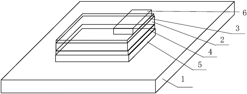
[0027] Such as figure 1 As shown, this embodiment is based on graphene / β-Ga 2 o 3 The Schottky junction deep ultraviolet light photodetector has the following structure: a metal copper sheet is used as a substrate 1, and β-Ga is fixed on the substrate 1 2 o 3 Single crystal and Schottky structure of graphene; β-Ga 2 o 3 The Schottky structure of single crystal and graphene is in β-Ga 2 o 3 The unpolished side of single wafer 2 is provided with β-Ga 2 o 3 Chromium / Au electrodes 4 in ohmic contact on a single wafer, on β-Ga 2 o 3 The polished surface of single wafer 2 is provided with β-Ga 2 o 3 A single wafer is a graphene film 3 in Schottky contact; the surface of the chromium / gold electrode 4 is uniformly coated with silver paste 5, so that the chromium / gold electrode 4 and the substrate 1 present a good ohmic contact; β-Ga 2 o3 The single wafer 2 and the substrate 1 are bonded by the silver paste 5; on one side of the graphene film 3, there is an extraction elect...


PUM

PropertyMeasurementUnit
thicknessaaaaaaaaaa
thicknessaaaaaaaaaa
currentaaaaaaaaaa

Abstract

The invention discloses a graphene / beta-Ga<2>O<3>-based schottky junction deep ultraviolet photodetector and a preparation method thereof. The deep ultraviolet photodetector is characterized in that with a metal copper sheet as a substrate, a schottky structure of a beta-Ga<2>O<3> single crystal wafer and graphene is fixed on the substrate; according to the schottky structure, a chromium / gold electrode is arranged on an unpolished surface of the beta-Ga<2>O<3> single crystal wafer and a graphene film is arranged on a polished surface; the surface of the chromium / gold electrode is evenly coated with silver paste; the beta-Ga<2>O<3> single crystal wafer and the substrate are bonded through the silver paste; and an extraction electrode is led out at one side of the graphene film. With a schottky junction formed by the beta-Ga<2>O<3> and the graphene as a core of a device, the deep ultraviolet photodetector disclosed by the invention can utilize the sensitivity of the beta-Ga<2>O<3> to a deep ultraviolet light and can also combine excellent characteristics of low resistivity, high transmittance and the like of the graphene. Therefore, the deep ultraviolet photodetector has high absorptivity on the deep ultraviolet light.

Description

technical field [0001] The invention relates to a deep ultraviolet light photodetector and a preparation method thereof, belonging to the application field of semiconductor device detection. Background technique [0002] Ultraviolet light is invisible light that resides in the high-energy region of sunlight. According to the wavelength, ultraviolet light is divided into: near ultraviolet light (UVA), far ultraviolet light (UVB) and ultra-short ultraviolet light (UVC). UVC is ultraviolet light with a wavelength of 280-100nm, which is completely absorbed by the ozone layer; UVB is ultraviolet light with a wavelength of 315-280nm; UVA is ultraviolet light with a wavelength of 400-315nm. Deep ultraviolet light photodetectors mainly detect ultraviolet light in the UVC band. Since the ultraviolet light in the UVC band reaching the ground is very small, this type of detector is also called a solar-blind detector. It is mainly used in flame detection, ultraviolet communication, mis...

Claims


Application Information

Patent Timeline
Patent Type & Authority Patents(China)
IPC IPC(8): H01L31/108H01L31/028H01L31/0296H01L31/18
CPCH01L31/028H01L31/0296H01L31/108H01L31/18Y02P70/50
Inventor 罗林保孔维玉张腾飞汪丹丹梁凤霞
Owner HEFEI UNIV OF TECH
Learn More