Ultraviolet avalanche photo-detector

A photodetector and ultraviolet avalanche technology, applied in the field of photoelectric detection, can solve the problems of high breakdown voltage and high cost, and achieve the effects of low breakdown voltage, low breakdown voltage and noise, and low voltage bias

Inactive Publication Date: 2016-06-08
UNIV OF ELECTRONICS SCI & TECH OF CHINA
View PDF4 Cites 15 Cited by
  • Summary
  • Abstract
  • Description
  • Claims
  • Application Information

AI Technical Summary

Problems solved by technology

[0006] Aiming at the inadequacies of the background, the present invention improves and designs an ultraviolet avalanche photodetector to solve the problem of high breakdown voltage and high cost of the photodetector in the prior art

Method used


Image

  • Ultraviolet avalanche photo-detector
  • Ultraviolet avalanche photo-detector
  • Ultraviolet avalanche photo-detector

Examples


Embodiment 1

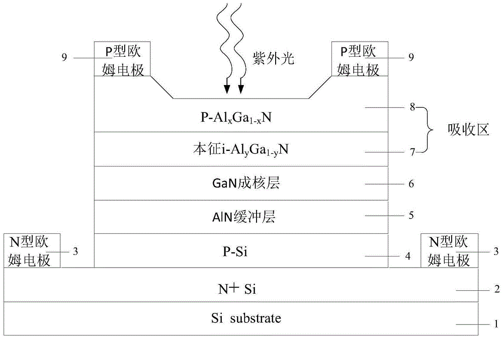
[0019] Such as figure 2 Shown is an ultraviolet avalanche photodetector, which includes from bottom to top: silicon substrate 1, N+ doped silicon 2, P type doped silicon 4, AlN buffer layer 5, GaN nucleation layer 6, intrinsic i- al y Ga 1-y N7, P-type doped P-Al x Ga 1-x N8, P-type ohmic electrode 9 and N-type ohmic electrode 3, wherein intrinsic i-Al y Ga 1-yN 7 and P-type doped P-Al x Ga 1-x N8 acts as an absorbing layer to absorb ultraviolet light, and P-type doped silicon 4 and N+ doped silicon 2 form a PN junction as a silicon-based avalanche region through photogenerated carriers (mainly electrons) to generate avalanche multiplication, thereby realizing the AlGaN absorption region and the separation of silicon-based multiplication regions.

[0020] In the device structure, from the silicon substrate 1 up, the thickness of the N+ doped silicon 2 is about 1 μm, and the concentration is at least 1×10 19 cm -3 , belonging to the high-concentration end of the PN j...

Embodiment 2

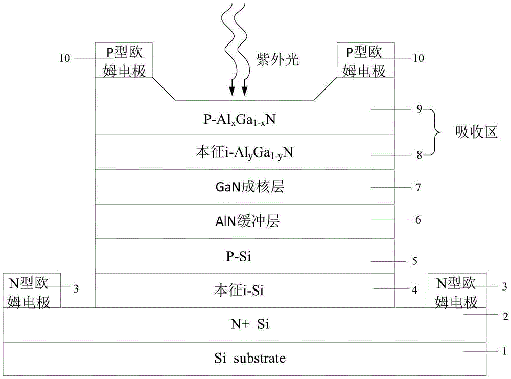
[0027] Such as image 3 Shown is an ultraviolet avalanche photodetector, which includes from bottom to top: silicon substrate 1, N+ doped silicon 2, intrinsic i-Si4, P-type doped silicon P-Si5, AlN buffer layer 6, GaN formed Core layer 7, intrinsic i-Al y Ga 1-y N8, P-type doped P-Al x Ga 1-x N9, P-type ohmic electrode 10 and N-type ohmic electrode 3, wherein intrinsic i-Al y Ga 1-y N8 and P-type doped P-Al x Ga 1-x N9 acts as an absorbing layer to absorb ultraviolet light. P-type doped silicon P-Si5, intrinsic i-Si4 and N+ doped silicon 2 form a PIN structure, which is used as a silicon-based avalanche region to generate photogenerated carriers (mainly electrons). Avalanche multiplication, thereby achieving the separation of the AlGaN absorption region and the silicon-based multiplication region.

[0028] In the device structure, from the silicon substrate 1 up, the thickness of the N+ doped silicon 2 is about 1 μm, and the concentration is at least 1×10 19 cm -3 , ...


PUM


Abstract

The invention provides an ultraviolet avalanche photo-detector which comprises a silicon substrate (1), a silicon-based avalanche layer (2), a buffering layer (3), a nucleating layer (4) and an absorbing layer (5) from bottom to top. Different from a conventional AlGaN material grows on sapphire or SiC substrate, the ultraviolet avalanche photo-detector is formed in the mode that the buffering layer and the nucleating layer grow on a silicon base, an AlGaN material serves as the absorbing layer, response to ultraviolet light wave bands is effectively improved, the silicon substrate is low in cost, large in single-crystal size and high in quality, and has small dark currents and low noise, and the avalanche layer is made of a silicon material and has low avalanche breakdown voltage. Ultraviolet light enters AlGaN in a normal incidence mode to excite photo-production electron-hole pairs, under action of an external electric field, a single current carrier (electrons) enters the silicon-based avalanche layer to trigger avalanche gain, an absorbing area and an avalanche area can be separated, and the ultraviolet avalanche photo-detector has low avalanche breakdown voltage, high gain, low noise and high bandwidth, and has a wide application range.

Description

technical field [0001] The invention relates to the field of photoelectric detection, in particular to a photoelectric detector. Background technique [0002] Due to its internal gain, the avalanche photodetector has the advantages of high sensitivity, low noise and high gain-bandwidth product, and can detect weak signals. It is widely used in optical fiber communication, laser ranging, single photon detection, and guidance technology. and other civilian and military fields. Studies have shown that the avalanche gain triggered by a single carrier (electron or hole) has less noise than the avalanche gain triggered by a double carrier. Furthermore, a single carrier with a larger impact ionization coefficient is used to Triggering an avalanche will bring relatively smaller noise and greater gain. Therefore, in silicon materials, using electrons with a higher impact ionization coefficient to trigger an avalanche will result in high gain and low noise. [0003] Generally, the s...

Claims


Application Information

Patent Timeline
Patent Type & Authority Applications(China)
IPC IPC(8): H01L31/107H01L31/0304
CPCH01L31/107H01L31/03044
Inventor 张有润袁福润刘影章志海张波
Owner UNIV OF ELECTRONICS SCI & TECH OF CHINA
Why Eureka
Try Eureka