Focused ion beam-electron beam fused controllable micro-nano machining method

A focused ion beam, micro-nano processing technology, applied in the fields of nanotechnology, nanotechnology, nanostructure manufacturing, etc., can solve the problem that it is difficult to control the precision and quality of FIB-SEM dual-beam synchronous processing, and it is difficult to control the dual-beam synchronous processing process. , affecting the quality of ion beam processing, etc., to achieve high-precision FIB-SEM dual-beam synchronous controllable processing, neutralization of local charge accumulation effects, and strong practicability.

Active Publication Date: 2016-06-15
BEIHANG UNIV
View PDF3 Cites 14 Cited by
  • Summary
  • Abstract
  • Description
  • Claims
  • Application Information

AI Technical Summary

Problems solved by technology

[0005] Among them, the disadvantages of the FIB single-beam system include: due to the accumulation of ion charges, the material of the sample will be greatly limited; compared with electrons, the mass of ions is much larger, and scanning ion imaging under the same energy and beam current will cause very little damage to the sample. large, which seriously affects the quality of ion beam processing; in addition, when scanning ion imaging, the number of secondary electrons generated is small, and it is difficult for general photomultiplier tube detectors to obtain sufficient secondary electron imaging, and more expensive micro The channel plate detector can only receive clear images
However, the above research simplifies the simultaneous processing of particles to atoms, ignoring the unneutralized ions and electrons in the FIB-SEM system. The processing performance only involves the interaction between atoms and samples, and the initial conditions such as the velocity of the incident atoms and the distribution of beam current density are too ideal. It is difficult to control the dual-beam synchronous processing process and improve the quality of FIB-SEM dual-beam synchronous processing
[0010] To sum up, in the existing FIB-SEM dual-beam synchronous system processing method, the types of incident particles of the sample are limited to ions or atoms, and the interaction mechanism between the synchronous beam and the sample fails to reflect the overall effect of ions, electrons, and atoms. The initial conditions such as particle velocity and beam density distribution on the surface are too ideal, and it is difficult to control the accuracy and quality of FIB-SEM dual-beam simultaneous processing

Method used


Image

  • Focused ion beam-electron beam fused controllable micro-nano machining method
  • Focused ion beam-electron beam fused controllable micro-nano machining method
  • Focused ion beam-electron beam fused controllable micro-nano machining method

Examples


Embodiment Construction

[0063] The present invention will be further described in detail with reference to the accompanying drawings and embodiments.

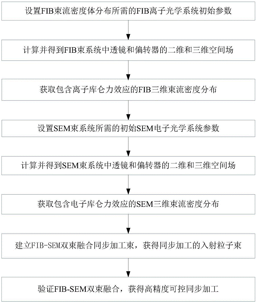
[0064] Since the incident processing beam spot in the FIB-SEM dual-beam synchronous system is small, on the order of nanometers, it is difficult to directly measure the parameters of the incident processing beam, such as velocity, beam density distribution, and incident angle, and is affected by the ion beam and Due to the double impact of electron beams, the types of incident beam particles involve atoms, ions and electrons. It is difficult to control the simultaneous processing of particle beams in existing methods. Therefore, a method of focused ion beam-electron beam dual-beam synchronous and controllable processing is proposed. See figure 1 , the specific operation steps are as follows:

[0065] First, according to the measured results of the dual-beam synchronization system independently integrated in the laboratory, the FIB ion optical system ...


PUM


Abstract

The invention discloses a focused ion beam-electron beam fused controllable micro-nano machining method, which is to obtain three-dimensional beam current density distribution of the ion beam and the electron beam respectively by comprehensively considering aberration and space charge effect of an actual system, and fuse the two beams according to the spatial layout of the system to synthesize a synchronous particle beam, so as to obtain high-precision two-beam fused controllable micro-nano machining. The method comprises the following steps: at first, obtaining parameters of a source, a lens, a deflector and a sample, and calculating two-dimensional fields, three-dimensional fields and electrical parameters of the lens and the deflector; then, under a given initial condition, solving Newton-Lorentz equation set to obtain ion (electron) beam three-dimensional beam current density distribution containing aberration and ion (electron) coulomb force effect; at last, under the condition of considering a two-beam system assembling structure, rotating the ion beam anticlockwise, fusing the ion beam and the electron beam under the coulomb force effect, so as to realize two-beam synchronous controllable machining. The method has the advantage that the machining precision and quality can be improved as the electron beam controls the ion beam current density distribution.

Description

technical field [0001] The invention belongs to the field of high-energy beam nano-in-situ processing and its real-time monitoring, and specifically relates to a method for controllable micro-nano processing of focused ion beam-electron beam double-beam fusion; Background technique [0002] Ion beam technology is the most compatible technology with semiconductor technology. Therefore, in the semiconductor integrated circuit manufacturing industry, ion beam technology has penetrated into many aspects of thin film production, material etching, impurity implantation, three-dimensional structure production and surface modification. Among them, the focused ion beam (FIB) is widely used in micro-nano-scale ion beam etching, ion beam deposition, ion implantation and ion beam material modification due to its high-resolution characteristics of high-energy particles and elemental properties. Focused ion beam technology is a microdissection technology that uses electrostatic lenses to ...

Claims


Application Information

Patent Timeline
Patent Type & Authority Applications(China)
IPC IPC(8): B82B3/00B82Y40/00
CPCB82B3/0004B82B3/0085B82Y40/00
Inventor 李文萍王荣明崔益民
Owner BEIHANG UNIV
Why Eureka
Try Eureka