

Laminated thin film solar battery and preparation method thereof
A solar cell and thin film technology, applied in circuits, photovoltaic power generation, electrical components, etc., can solve problems such as inability to adjust current flow and light transmittance, long-term battery stability risks, poor transmittance, etc. Facilitate optical transmission and resistivity, wide application range, and large absorption range
- Summary
- Abstract
- Description
- Claims
- Application Information
AI Technical Summary
Problems solved by technology
Method used
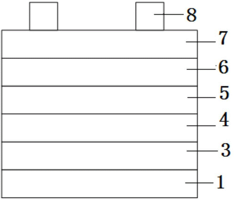
Image

Examples
Embodiment 1
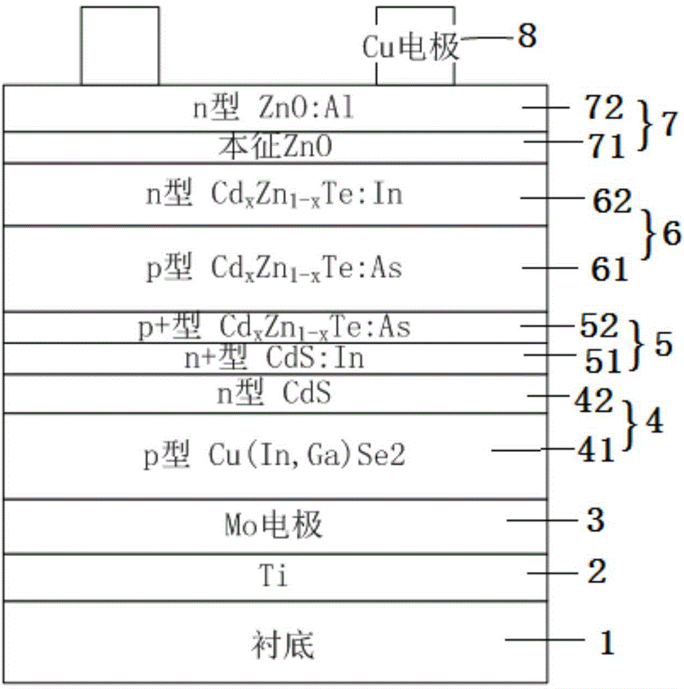
[0043] [101] Form the back electrode 3 on the substrate 1 by magnetron sputtering method, and its preparation thickness is 500nm;
[0044] [102] Form the p-type semiconductor layer 41 of the bottom cell 4 on the back electrode 3 by magnetron sputtering or co-evaporation, that is, P-type Cu(In, Ga)Se 2 A semiconductor layer with a thickness of 500nm and a doping concentration of 1x10 17 cm -3 , with a band gap of 1.0eV, using Cu, In, Ga alloy targets, forming p-type Cu(In,Ga)Se at a pressure of 0.1Pa and a Se atmosphere 2 Absorption layer of semiconductor material, in which Cu / (In+Ga):Ga / (In+Ga) of the alloy target has a gradient change, which can be optimized according to the process performance.
[0045] [103] On the p-type semiconductor layer 41 of the bottom cell 4, form the n-type semiconductor layer 42 of the bottom cell 4 by magnetron sputtering or a chemical water bath, that is, the n-type CdS buffer layer, using a CdS target at a pressure of 0.1 Pa, Ar, O 2 , H 2 ...
Embodiment 2
[0051] [201] On a metal foil substrate 1 with a thickness of 50 μm, a metal titanium barrier layer 2 with a thickness of 500 nm was prepared by magnetron sputtering using a metal titanium target at a gas pressure of 10 Pa and argon as a process gas.
[0052] [202] On the metal titanium barrier layer 2, molybdenum target with a thickness of 700nm was prepared as the back electrode 3 by using a molybdenum target at a gas pressure of 10Pa and argon as the process gas by magnetron sputtering.
[0053] [203] On the back electrode 3, by means of magnetron sputtering, Cu, In, Ga alloy targets are used to form p-type Cu(In, Ga)Se at a pressure of 10Pa and a Se atmosphere. 2 semiconductor layer. The Cu / (In+Ga):Ga / (In+Ga) of the alloy target has a gradient change, which can be optimized according to the process performance. Cu(In,Ga)Se 2 The thickness of semiconductor material is 2000nm. The doping concentration is 1x10 17 cm -3 , with a bandgap of 1.2eV.
[0054] [204] On the p-t...
Embodiment 3
[0061] [301] On a stainless steel substrate 1 with a thickness of 40 μm, a metal titanium barrier layer 2 with a thickness of 400 nm was prepared by magnetron sputtering using a metal titanium target at a pressure of 5 Pa and the process gas being argon.
[0062] [302] On the metal titanium barrier layer 2, molybdenum target with a thickness of 600nm was prepared as the back electrode 3 by magnetron sputtering at a gas pressure of 5Pa and argon gas as the process gas.
[0063] [303] On the back electrode 3, by means of magnetron sputtering, Cu, In, Ga alloy targets are used to form p-type Cu(In, Ga)Se at a pressure of 6Pa and a Se atmosphere. 2 semiconductor layer. The Cu / (In+Ga):Ga / (In+Ga) of the alloy target changes in a gradient. The Cu(In,Ga)Se2 semiconductor material has a thickness of 1000nm and a doping concentration of 1x10 17 cm -3 , with a bandgap of 1.1eV.
[0064] [304] On the p-type semiconductor layer 41 of the bottom cell 4, a CdS target is used, at a pressu...
PUM
 Abstract
Description
Claims
Application Information