Method for preparing black silicon on doped film layer

A technology of doping silicon and black silicon, which is applied in the manufacture of final products, sustainable manufacturing/processing, electrical components, etc., and can solve the problems of cumbersome wet etching steps, toxic waste gas, waste liquid, and low shape accuracy , to achieve the effect of enriching the types of doping elements, increasing the doping concentration and reducing the cost of doping

Inactive Publication Date: 2016-07-06
UNIV OF ELECTRONICS SCI & TECH OF CHINA
View PDF7 Cites 6 Cited by
  • Summary
  • Abstract
  • Description
  • Claims
  • Application Information

AI Technical Summary

Problems solved by technology

However, the wet etching steps are cumbersome, the obtained morphology is not accurate, the size is small, and it will produce toxic waste gas and waste liquid.

Method used


Image

  • Method for preparing black silicon on doped film layer
  • Method for preparing black silicon on doped film layer
  • Method for preparing black silicon on doped film layer

Examples


Embodiment Construction

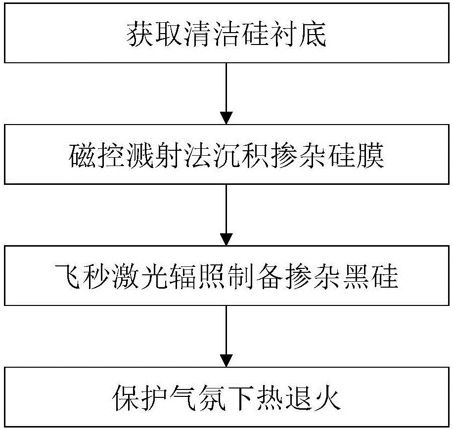
[0022] The present invention will be described in detail below in conjunction with the drawings.

[0023] Such as figure 1 As shown, the preparation of the doped black silicon material in the present invention is to prepare the doped black silicon microstructure by means of femtosecond laser irradiation after preparing the doped film. The specific steps are as follows:

[0024] Step 1: Obtain a clean silicon substrate

[0025] A silicon substrate with a size of 10 mm×10 mm was sonicated for 15 minutes in each of the three solutions in sequence to wash off the oil, particles and oxides on the surface of the substrate. The three solutions are: No. I cleaning solution is concentrated sulfuric acid (H 2 SO 4 ) And 9.7mol / L hydrogen peroxide (H 2 O 2 ), the volume ratio is 5:1; the cleaning solution II is deionized water (H 2 O), hydrogen peroxide (H 2 O 2 ) And 13.3mol / L ammonia (NH 3 ·H 2 O), the volume ratio is 5:2:1; the cleaning solution III is deionized water (H 2 O), the concentrat...


PUM

PropertyMeasurementUnit
thicknessaaaaaaaaaa

Abstract

The invention relates to the field of a semiconductor photoelectronic material, is applied to the preparation of doped black silicon, and specifically discloses a method for preparing a doped black silicon microstructure through a femtosecond laser radiation method after the doped film layer is prepared. According to the preparation method, a target material fitting mode and a magnetron sputtering method are adopted to deposit a silicon-doped film layer on the surface of a clean silicon substrate; then a surface microstructure is prepared through femtosecond laser radiation; the surface microstructure is thermally annealed under an atmosphere environment to obtain the doped black silicon material, wherein the doped black silicon material has a certain high absorption characteristic on light with the wavebands of 400-2,400nm; the absorption rate of the doped black silicon material on the visible light wavebands of 400-1,100nm can reach 95%, and the absorption rate of the doped black silicon material on the near infrared wavebands of 1,100-2,400nm can reach 90%, so that technological foundation for expanding the application of the black silicon material is established. Compared with the prior art, the types of the doped elements are enriched due to the solid film layer doping mode; and meanwhile, the doping concentration is improved, the doping cost is lowered, the process steps are reduced, and the preparation efficiency is improved.

Description

Technical field [0001] The invention relates to the field of semiconductor optoelectronic materials and is applied to the preparation of doped black silicon. Specifically, after preparing the doped film layer, the doped black silicon microstructure is prepared by femtosecond laser irradiation. Background technique [0002] As an important semiconductor material with low cost and easy integration, silicon material occupies a leading position in the field of microelectronics and optoelectronics. Devices and products made from it have been widely used in fields such as computers, communications, information technology, and energy technology. . However, due to its own band gap restriction, its application in optoelectronic devices is limited. Specifically, because crystalline silicon does not absorb light with a wavelength greater than 1100nm (the absorption coefficient is less than 100cm -1 ), resulting in low response rate of infrared detectors and low conversion efficiency of ph...

Claims


Application Information

Patent Timeline
Patent Type & Authority Applications(China)
IPC IPC(8): H01L31/18H01L31/0288H01L31/0236
CPCH01L31/02363H01L31/0288H01L31/1804Y02P70/50
Inventor 吴志明李睿杜玲艳唐菲胡征李世彬李伟吴雪飞姬春晖
Owner UNIV OF ELECTRONICS SCI & TECH OF CHINA
Why Eureka
Try Eureka