Silicon carbide MOSFET device and manufacturing method thereof

A technology of silicon carbide and devices, which is applied in semiconductor/solid-state device manufacturing, semiconductor devices, electrical components, etc., can solve problems such as device thermal burnout, device or ion implanter pollution, current amplification, etc., to suppress turn-on and improve anti-UIS The effect of incapacity

Inactive Publication Date: 2016-07-13
UNIV OF ELECTRONICS SCI & TECH OF CHINA
View PDF4 Cites 14 Cited by
  • Summary
  • Abstract
  • Description
  • Claims
  • Application Information

AI Technical Summary

Problems solved by technology

The metal mask may contaminate the device or the ion implanter to a certain extent during high-temperature ion implantation, which we do not want to see
[0005] During the UIS test, a large voltage and current will be generated at the drain-source terminal of the MOSFET. If the avalanche current generates a sufficiently large voltage drop on the base resistance of the parasitic transistor, the parasitic transistor will be turned on and the current will be further amplified. Ultimately causing thermal burnout of the device

Method used


Image

  • Silicon carbide MOSFET device and manufacturing method thereof
  • Silicon carbide MOSFET device and manufacturing method thereof
  • Silicon carbide MOSFET device and manufacturing method thereof

Examples


Embodiment Construction

[0043] The embodiments of the present invention are described below through specific specific examples, and those skilled in the art can easily understand other advantages and effects of the present invention from the contents disclosed in this specification. The present invention can also be implemented or applied through other different specific embodiments, and various details in this specification can also be modified or changed based on different viewpoints and applications without departing from the spirit of the present invention.

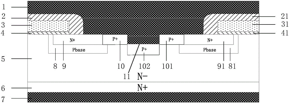
[0044]A silicon carbide MOSFET device, comprising a drain metal 7, an N+ substrate 6 above the drain metal 7, and an N-drift region 5 above the N+ substrate 6; the N-drift region 5 is provided with a recess in the middle above the interior The groove 11, the left side of the groove 11 is the first P-type base region 8, and the right side is the second P-type base region 81; the first N+ source region 9 is arranged above the inside of the firs...


PUM

PropertyMeasurementUnit
lengthaaaaaaaaaa

Abstract

The invention provides a silicon carbide MOSFET device and a manufacturing method thereof. The device comprises a drain electrode metal unit, an N+ substrate, and an N- drift region. And a groove is formed in the N- drift region. Besides, the manufacturing method includes: a groove is etched in an epitaxial wafer, wherein the groove and a lithography aligning mark are formed simultaneously; polysilicon is deposited on an N- epitaxy unit and etching is carried out to form an ion implantation barrier layer pattern; aluminium ion implantation is carried out by using the polysilicon as a mask to form a P type base region; silicon dioxide is deposited and back etching is carried out to form a side wall, and nitrogen ion implantation is carried out by using a self-aligning technology to form an N+ source region; the polysilicon and silicon dioxide are removed, and polysilicon is deposited and an ion implantation barrier layer pattern is formed; aluminium ion implantation is carried out to form a P+ contact region; and the polysilicon is removed, ion implantation activation annealing and gate oxide oxidation are carried out. According to the invention, the channel self-aligning technology is realized and the depth of the P+ contact region is increased, so that the starting of the parasitic BJT transistor is suppressed effectively and the anti-UIS failure capability of the silicon carbide MOSFET device is enhanced to a certain extent.

Description

technical field [0001] The invention belongs to the technical field of power semiconductors, in particular to a silicon carbide MOSFET device and a manufacturing method thereof involving a channel self-alignment process. Background technique [0002] As one of the representatives of the third-generation wide-bandgap semiconductor materials, silicon carbide (SiliconCarbide) material has the characteristics of large band gap, high critical breakdown electric field, high thermal conductivity and high electron saturation drift speed, making it suitable for high-power, High temperature and high frequency power electronics have broad application prospects. [0003] Silicon carbide MOSFETs have low on-resistance and low switching losses, and are more suitable for high-frequency operation. In addition, they also have excellent electrical characteristics in high temperature regions, and have gradually become a new generation of mainstream low-loss power devices. [0004] Reducing th...

Claims


Application Information

Patent Timeline
Patent Type & Authority Applications(China)
IPC IPC(8): H01L29/06H01L29/24H01L21/336H01L29/78
CPCH01L29/0684H01L29/24H01L29/66068H01L29/78
Inventor 邓小川陈茜茜李立均李轩张波
Owner UNIV OF ELECTRONICS SCI & TECH OF CHINA
Why Eureka
Try Eureka