Ferroelectric field effect transistor based on GeSn material, and preparation method for ferroelectric field effect transistor

An electric field effect and transistor technology, applied in the field of electronics, can solve the problems of reduced operating voltage, low electron mobility, and high power consumption of transistors, and achieve the effects of reducing device delay, high electron mobility, and low subthreshold swing.

Inactive Publication Date: 2016-07-13
XIDIAN UNIV
View PDF7 Cites 5 Cited by
  • Summary
  • Abstract
  • Description
  • Claims
  • Application Information

AI Technical Summary

Problems solved by technology

However, the disadvantage of the MFIS-FET structure is that the electron mobility of silicon, the material used for the substrate, is low, which leads to a small conduction current of the transistor, and it becomes difficult to further reduce the subthreshold swing. Therefore, the switching speed of the transistor cannot be increased, and the application requirements of high-performance devices cannot be met.
However, there are still deficiencies that the transistor cannot reduce the operating voltage while increasing the conduction current of the transistor, resulting in high power consumption of the transistor, and cannot reduce the subthreshold swing and increase the switching speed of the transistor.

Method used


Image

  • Ferroelectric field effect transistor based on GeSn material, and preparation method for ferroelectric field effect transistor
  • Ferroelectric field effect transistor based on GeSn material, and preparation method for ferroelectric field effect transistor
  • Ferroelectric field effect transistor based on GeSn material, and preparation method for ferroelectric field effect transistor

Examples


Embodiment 1

[0055] Embodiment 1: making Ge 0.935 sn 0.065 P-type ferroelectric field effect crystal.

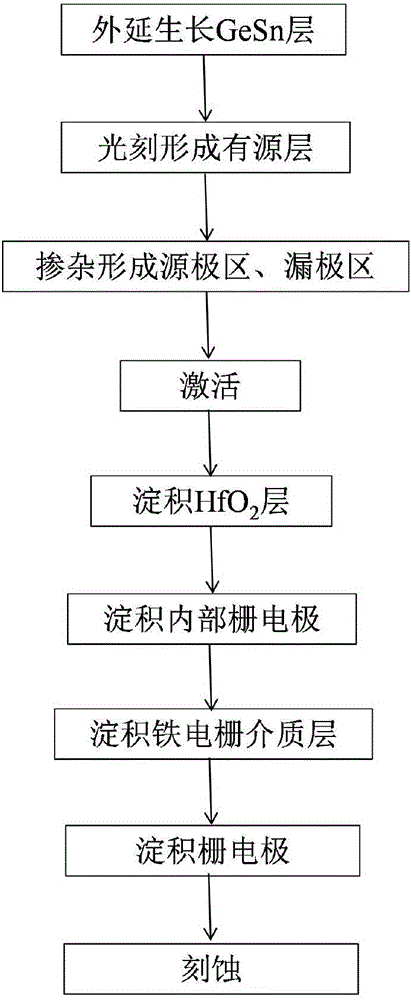
[0056] Step 1. Epitaxially grow a GeSn layer.

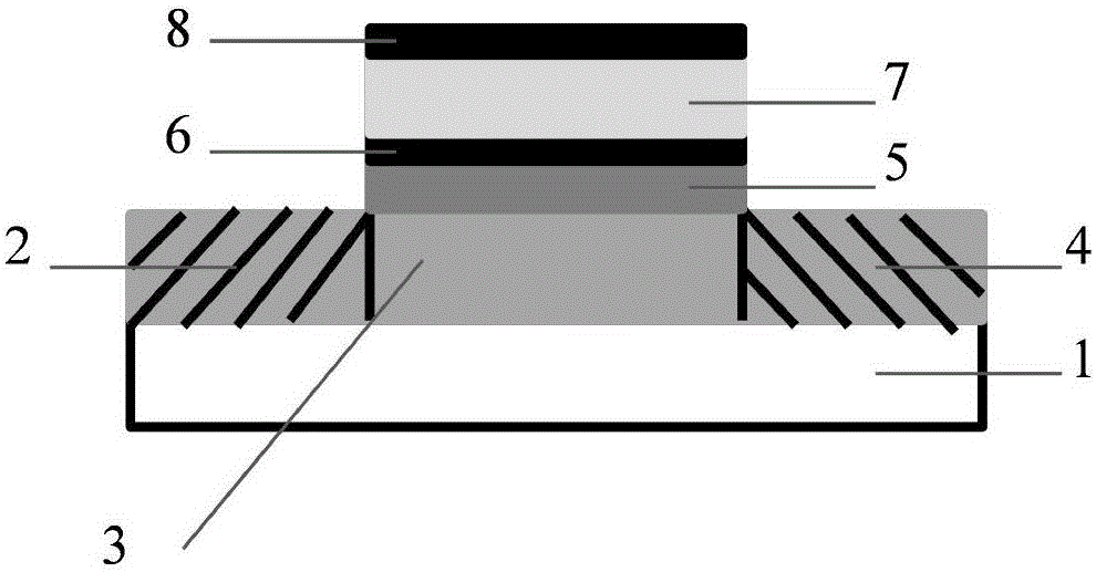
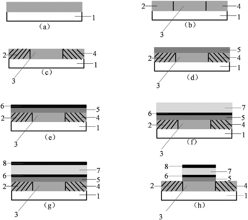
[0057] Using low-temperature solid-source molecular beam epitaxy, epitaxially grow 80nm Ge on undoped Ge substrates with high-purity Ge and Sn sources at 180°C 0.935 sn 0.065 layer. image 3 (a) For epitaxial growth of Ge 0.935 sn 0.065 Schematic diagram of the result after layers.

[0058] Step 2. Form the active layer by photolithography.

[0059] Using a 365nm I-line photolithography process, a source layer, a channel and a drain layer are formed on the GeSn layer, wherein the channel is located in the center of the GeSn layer, and the source layer and drain layer are located on both sides of the channel. image 3 (b) is a schematic diagram of the result after forming the source layer, channel and drain layer.

[0060] Step 3. Doping to form a source region and a drain region.

[0061] The implant energy in the source and drain...

Embodiment example 2

[0072] Implementation Case 2: Making Ge 0.935 sn 0.065 N-type ferroelectric field effect crystal.

[0073] Step 1. Epitaxial growth of a GeSn layer.

[0074] Using low-temperature solid-source molecular beam epitaxy, epitaxially grow 80nm Ge on undoped Ge substrates with high-purity Ge and Sn sources at 180°C 0.935 sn 0.065 layer. image 3 (a) For epitaxial growth of Ge 0.935 sn 0.065 Schematic diagram of the result after layers.

[0075] Step 2. Forming an active layer by photolithography.

[0076] Using a 365nm I-line photolithography process, a source layer, a channel and a drain layer are formed on the GeSn layer, wherein the channel is located in the center of the GeSn layer, and the source layer and drain layer are located on both sides of the channel. image 3 (b) is a schematic diagram of the result after forming the source layer, channel and drain layer.

[0077] Step 3. Doping to form a source region and a drain region.

[0078] The implantation energy in t...

Embodiment example 3

[0089] Implementation Case 3: Making Ge 0.9 sn 0.1 P-type ferroelectric field effect crystal.

[0090] Step a. epitaxially growing a GeSn layer.

[0091] Using low-temperature solid-source molecular beam epitaxy, epitaxially grow 80nm Ge on undoped Ge substrates with high-purity Ge and Sn sources at 180°C 0.9 sn 0.1 layer. image 3 (a) For epitaxial growth of Ge 0.9 sn 0.1 Schematic diagram of the result after layers.

[0092] Step b. Forming the active layer by photolithography.

[0093] Using a 365nm I-line photolithography process, a source layer, a channel and a drain layer are formed on the GeSn layer, wherein the channel is located in the center of the GeSn layer, and the source layer and drain layer are located on both sides of the channel. image 3 (b) is a schematic diagram of the result after forming the source layer, channel and drain layer.

[0094]Step c. Doping to form a source region and a drain region.

[0095] The implant energy in the source and dra...


PUM


Abstract

The invention discloses a ferroelectric field effect transistor based on a GeSn material, and a preparation method for the ferroelectric field effect transistor, and solves problems that a conventional ferroelectric field effect transistor is small in conduction current and is larger in subthreshold swing. The ferroelectric field effect transistor comprises a substrate 1, a source electrode 2, a trench 3, a drain electrode 4, an insulating dielectric film 5, an internal grid electrode 6, a ferroelectric grid dielectric layer 7, and a grid electrode 8. The trench 3 is located at the center above the substrate 1, and the source electrode 2 and the drain electrode 4 are located at two sides of the trench 3. The insulating dielectric film 5, the internal grid electrode 6, the ferroelectric grid dielectric layer 7 and the grid electrode 8 are sequentially distributed above the trench 3 from the bottom to the top in a vertical manner. According to the invention, the GeSn material is introduced as the trench material of the transistor, thereby enabling the transistor to be able to obtain a smaller subthreshold swing and a higher switching speed at a low working voltage.

Description

technical field [0001] The invention belongs to the technical field of electronics, and further relates to a GeSn material-based ferroelectric field effect transistor and a preparation method thereof in the technical field of microelectronic devices. The invention can be used in large-scale integrated circuits with high performance and low power consumption. Background technique [0002] With the development of integrated circuits, the feature size of chips has been continuously reduced, and the integration level on a single chip has increased accordingly, and the resulting power consumption problem has become more and more serious. According to ITRS data, when the feature size is reduced to the 32nm node, the power consumption will be 8 times the expected trend, that is, with the gradual reduction of the feature size, traditional MOS devices will not be able to meet the performance requirements in terms of power consumption. In addition, the reduction of MOSFET size is lim...

Claims


Application Information

Patent Timeline
Patent Type & Authority Applications(China)
IPC IPC(8): H01L29/08H01L29/10H01L29/417H01L21/336
CPCH01L29/6684H01L29/0847H01L29/1033H01L29/41725
Inventor 张春福韩根全彭悦郝跃张进城冯倩
Owner XIDIAN UNIV
Why Eureka
Try Eureka