
Parameter extraction method for small-signal circuit model of gallium nitride high electron mobility transistor

A high electron mobility and circuit model technology, applied in the field of microelectronics, can solve problems such as device damage, extraction of parasitic inductance, resistance error, and dependence, and achieve the effects of improving reference efficiency, applicable frequency bandwidth, and reducing errors

Active Publication Date: 2019-01-08
XIDIAN UNIV
View PDF5 Cites 0 Cited by
  • Summary
  • Abstract
  • Description
  • Claims
  • Application Information

AI Technical Summary

Problems solved by technology

Therefore, this extraction method will cause inaccuracy in extracting the peripheral PAD capacitance, which will cause errors in the subsequent extraction of parasitic inductance and resistance, and manual tuning is more troublesome and not suitable for modeling large-scale devices
When extracting parasitic inductance, it is necessary to re-measure another set of scattering parameters for extraction. At this time, the device needs to work under the condition of positive large gate voltage, which will also cause certain damage to the device.
[0006] The above optimization search method does not need to make assumptions about the physical structure of the device, and the accuracy of the parameters is high, but the extraction of parameters requires a lengthy and complex iterative algorithm, and the accuracy of the process is very dependent on the selection of appropriate initial values ​​and the final extracted values There is no physical meaning inconsistent with the actual physical structure of the device

Method used


Image

  • Parameter extraction method for small-signal circuit model of gallium nitride high electron mobility transistor
  • Parameter extraction method for small-signal circuit model of gallium nitride high electron mobility transistor
  • Parameter extraction method for small-signal circuit model of gallium nitride high electron mobility transistor

Examples


Embodiment Construction

[0040] The principles and features of the present invention are described below in conjunction with the accompanying drawings, and the examples given are only used to explain the present invention, and are not intended to limit the scope of the present invention.

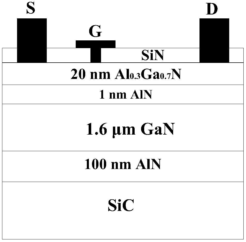
[0041] refer to figure 1 , the existing GaN HEMT device consists of a 2-inch 4H-SiC substrate from bottom to top, a 100nm thick AlN nucleation layer, a 1.6um thick GaN buffer layer, a 1nm AlN insertion layer, and a 20nm undoped AlGaN barrier layer, 60nm SiN passivation layer, Ti / Al / Ni / Au ohmic source electrode and ohmic drain electrode and Ni / Au / Ni Schottky gate, the gate width of the device is 10x125um, the gate length is 0.4um, gate-gate , Gate-source, gate-drain spacing are 40um, 0.7um and 2.8um respectively.

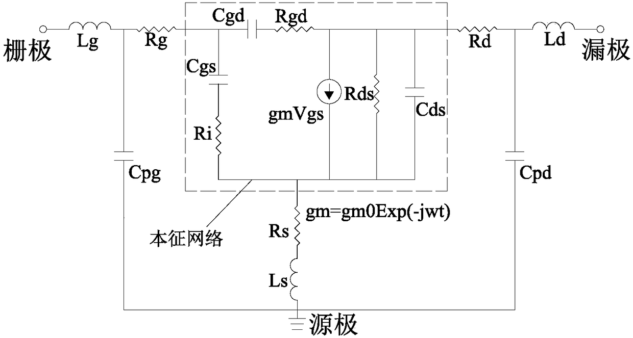
[0042] figure 1 The small-signal equivalent circuit diagram of the device structure shown is figure 2 As shown, it includes 16 circuit components, which are divided into two categories, namely peripher...


PUM


Abstract

The invention discloses a GaN HEMT (high electron mobility transistor) small signal circuit model parameter extraction method and mainly solves the problems that a device is damaged due to forward high gate voltage during extraction of parasitic inductance, manual tuning is needed during extraction of the parasitic inductance and optimized parameters do not meet a physical structure in the prior art. According to the technical scheme, on the basis of traditional extraction of the parasitic inductance, the parasitic inductance is introduced into an equivalent circuit in a low-frequency cold-bias cutoff state, total parasitic capacitance and the parasitic inductance are extracted simultaneously with a linear regression method, parasitic capacitance is optimally searched out through combination of an actual physical structure, and parasitic resistance and intrinsic parameters are extracted out through combination of scattering parameters tested under a non-bias condition and scattering parameters during normal working. According to the method, the device is not damaged in a test process, manual tuning is not needed, the extraction efficiency of the parameters is higher, and the method is suitable for the frequency band width; the model parameters obtained with the method not only can be directly used for establishing a small signal equivalent circuit model of the device, but also can be used for small signal circuit design.

Description

technical field [0001] The invention belongs to the technical field of microelectronics, in particular to a GaN HEMT transistor model parameter extraction method, which can be used in radio frequency integrated circuit design. technical background [0002] AlGaN / GaN high electron mobility transistor (HEMT) has increasingly become the focus of today's RF microwave circuit design due to its characteristics of high power, high current density, high electron saturation velocity and high breakdown electric field. As the miniaturization of integrated circuits continues to increase and the degree of integration continues to increase, people's enthusiasm for the design of monolithic microwave integrated circuits (MMICs) is gradually increasing. Accurate device models play a crucial role in the design and evaluation of MMIC circuits. In the whole modeling process, the small-signal model of the transistor is the basis of the large-signal model, so the establishment of the small-signa...

Claims


Application Information

Patent Timeline
Patent Type & Authority Patents(China)
IPC IPC(8): G06F17/50
CPCG06F17/12G06F30/30
Inventor 马晓华张恒爽马佩军郑佳欣卢阳赵博超郝跃
Owner XIDIAN UNIV
Learn More