Semiconductor device and preparation method thereof and electronic device

A technology for semiconductors and devices, applied in the field of semiconductor manufacturing, can solve problems such as failure, device performance and yield reduction, sidewall damage, etc.

Active Publication Date: 2016-07-20
SEMICON MFG INT (SHANGHAI) CORP
View PDF4 Cites 0 Cited by
  • Summary
  • Abstract
  • Description
  • Claims
  • Application Information

AI Technical Summary

Problems solved by technology

[0005] Part of the sidewall of the floating gate structure obtained after the conventional COPEN step is vertical, and the sidewall is damaged during the etching process, which affects the storage capacity of the semiconductor device, making the The programming speed of semiconductor devices is reduced, and even fails
[0006] In addition, with the continuous shrinking of the size of semiconductor devices, the stability of the device has become the most important factor for device safety.

Method used


Image

  • Semiconductor device and preparation method thereof and electronic device
  • Semiconductor device and preparation method thereof and electronic device
  • Semiconductor device and preparation method thereof and electronic device

Examples


preparation example Construction

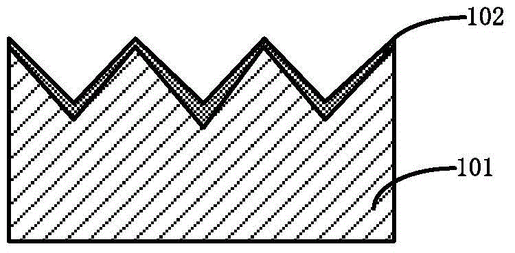
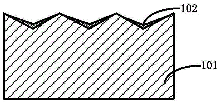
[0040]The current manufacturing method of the semiconductor device includes the following steps: firstly providing a semiconductor substrate, forming a floating gate material layer and a hard mask layer on the semiconductor substrate, then patterning the hard mask layer (HMetch), and Etching the floating gate material layer using the hard mask layer as a mask to form a floating gate structure, then depositing an ALD oxide layer to form an oxide layer on the sidewall of the floating gate structure, and then using the The hard mask layer and the floating gate structure are used as masks to etch the semiconductor substrate to form shallow trenches in the semiconductor substrate, and then the shallow trench isolation materials are selected to fill the shallow trenches and planarized to form a shallow trench isolation structure, and then remove the hard mask layer, and then perform a step of opening (cellopen, COPEN) a memory cell to remove part of the oxide in the shallow trench is...

Embodiment 1

[0043] In order to solve the problems existing in the prior art, the present invention improves the manufacturing process steps of the semiconductor device and the parameters in the steps, so as to eliminate the above-mentioned problems, the preparation method of the semiconductor device of the present invention is further described below illustrate.

[0044] First, step 201 is performed to provide a semiconductor substrate, on which a floating gate material layer and a hard mask layer are sequentially formed.

[0045] Specifically, wherein, the semiconductor substrate may be at least one of the materials mentioned below: silicon, silicon-on-insulator (SOI), silicon-on-insulator (SSOI), silicon-germanium-on-insulator (S- SiGeOI), silicon germanium on insulator (SiGeOI) and germanium on insulator (GeOI), etc.

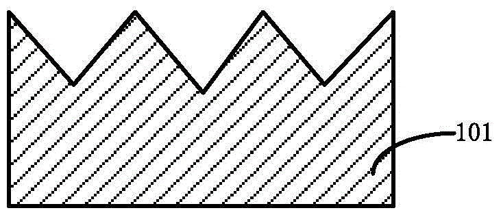
[0046] A floating gate material layer and a mask layer are formed on the semiconductor substrate and patterned to form a floating gate structure and a shallow trench. ...

Embodiment 2

[0091] The present invention also provides a semiconductor device, which is prepared by the method described in Embodiment 1. The sidewall of the floating gate structure in the semiconductor device prepared by the method of the present invention is not damaged, and the sidewall of the floating gate structure is smoother, which improves the coupling performance with the subsequently formed control gate structure, and further Improve device performance and yield.


PUM


Abstract

The invention relates to a semiconductor device and a preparation method thereof and an electronic device. The method comprises the following steps: (S1) providing a semiconductor substrate, forming a plurality of floating gate structures on the semiconductor substrate, forming shallow trench isolation structures which extend to the semiconductor substrate downwards between the adjacent floating gate structures; (S2) etching back and removing partial isolated oxides in the shallow trench isolation structures to expose the side walls of the floating gate structures; and (S3) etching the side walls of the floating gate structures by a chemical downstream etching method to make the side walls of the floating gate structures smooth and uniform. The side walls of the floating gate structures prepared by the method are relatively smooth; the LER performance between the floating gate structures is greatly improved; and meanwhile, the floating gate structures are relatively uniform, so that the coupling performance with the subsequently formed control gate structure is improved; and the performance and the yield of the device are further improved.

Description

technical field [0001] The invention relates to the field of semiconductor manufacturing, and in particular, the invention relates to a semiconductor device, a preparation method thereof, and an electronic device. Background technique [0002] With the increasing demand for high-capacity semiconductor storage devices, the integration density of these semiconductor storage devices has received more attention. In order to increase the integration density of semiconductor storage devices, many different methods have been adopted in the prior art, such as through Reducing the size of the memory cell and / or changing the structure of the unit to form more memory cells on a single wafer, as for the method of increasing the integration density by changing the cell structure, attempts have been made by changing the planar layout of the active region or changing Cell layout to reduce cell area. [0003] NAND flash memory is a better storage solution than hard disk drives. Since NAND ...

Claims


Application Information

Patent Timeline
IPC IPC(8): H01L21/8247H01L21/28H01L27/115
Inventor 张翼英任佳
Owner SEMICON MFG INT (SHANGHAI) CORP
Why Eureka
Try Eureka