VDMOS device with variable dielectric side

A medium and device technology, applied in the field of semiconductor power devices, can solve problems such as limited electric field modulation

Inactive Publication Date: 2016-07-20
XIDIAN UNIV
View PDF4 Cites 6 Cited by
  • Summary
  • Abstract
  • Description
  • Claims
  • Application Information

AI Technical Summary

Problems solved by technology

But its modulation of the electric field is limited, and there is still room for improvement

Method used


Image

  • VDMOS device with variable dielectric side
  • VDMOS device with variable dielectric side
  • VDMOS device with variable dielectric side

Examples


Embodiment Construction

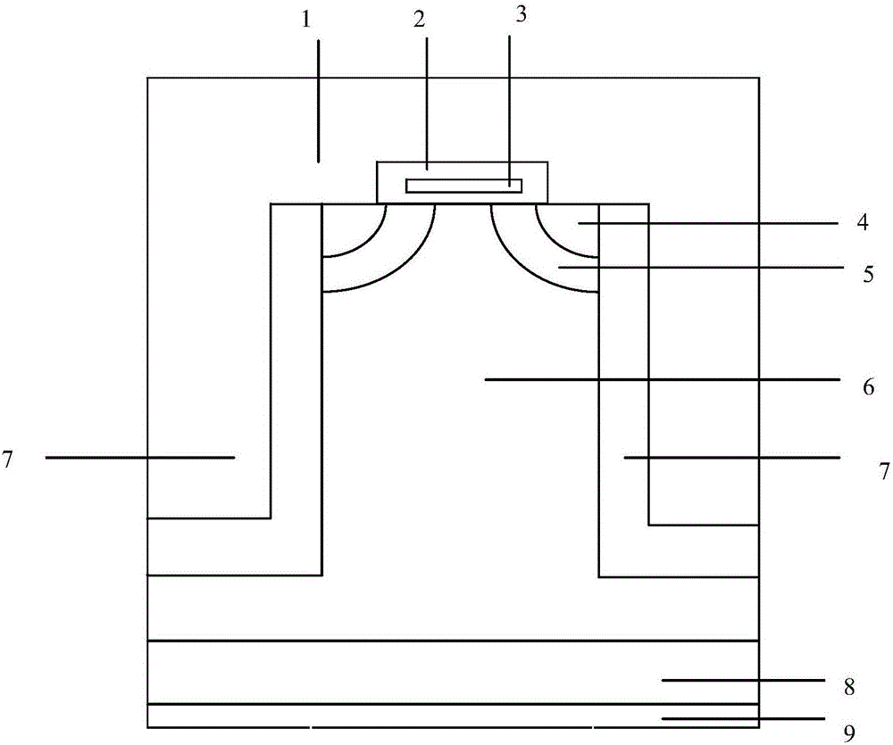
[0026] The new structure mainly includes side layers filled with a variety of dielectrics with different dielectric constants (K values), polysilicon trenches, isolation dielectrics, P-type (N-type) base regions, N-type (P-type) drift regions, and N-type (P-type) substrate. Such as image 3 As shown, an N-channel VDMOS device is taken as an example to further illustrate the specific implementation of the present invention.

[0027] The N-channel VDMOS device includes a source 1, an isolation medium 2, a gate 3, an N+ source region 4, a P-type base region 5, an N-drift region 6, an N+ substrate 8 and a drain metal 9, and is characterized by: It also has a side layer 7 formed by sequentially filling a plurality of different K-value media, and the side layer 7 formed by sequentially filling a plurality of different K-value media is located on both sides of the N-drift zone.

[0028] By sequentially filling the side layers composed of a variety of different K-value media to generate n...


PUM


Abstract

The invention discloses a VDMOS device with a variable dielectric side. A new electric field peak is generated by sequentially filling side layers formed by dielectrics with different dielectric constants (K value), the field distribution of VDMOS high resistance drift region is modulated, and the lateral electric field modulation effect is enhanced, so that high-density doping can be conducted on the drift region. Under same breakdown voltage conditions, the structure makes the VDMOS have lower specific on-resistance. The novel structure can increase the breakdown voltage of the device and lower the conduction resistance of the power device. A new technology breaking the silicon limit of a power device is provided.

Description

Technical field [0001] The invention belongs to the technical field of semiconductor power devices, and specifically relates to a VDMOS structure. Background technique [0002] Power Metal-Oxide-SemiconductorFieldEffectTransistor (MOSFET) is a new generation of power switching devices developed on the basis of MOS integrated circuit technology. VDMOS devices have a series of unique characteristics such as high input impedance, fast switching speed, high operating frequency, voltage control, and good thermal stability. At present, they have been obtained in the aspects of switching steady-state power supplies, high-frequency heating, computer interface circuits, and power amplifiers. Wide range of applications. [0003] In order to meet the function of switching, the power MOSFET should meet two important requirements: when the device is in the on state, it has a sufficiently low on-resistance to reduce the conduction loss, and when the device is in the off state, it maintains a ce...

Claims


Application Information

Patent Timeline
Patent Type & Authority Applications(China)
IPC IPC(8): H01L29/06H01L29/78
CPCH01L29/7802H01L29/06
Inventor 袁嵩段宝兴蔡海杨银堂
Owner XIDIAN UNIV
Why Eureka
Try Eureka