PCB pad compensation design technology and application thereof

A PCB board and design process technology, applied in the field of PCB board pad compensation design process, can solve the problems of different sizes, low feasibility, restricting the improvement of product quality, etc., to achieve uniform shape of the pads, avoid virtual welding, The effect of improving production yield

Active Publication Date: 2016-07-20
PLOTECH TECH KUNSHAN CO LTD
View PDF3 Cites 11 Cited by
  • Summary
  • Abstract
  • Description
  • Claims
  • Application Information

AI Technical Summary

Problems solved by technology

However, since the circuit 41 is obtained by etching the copper layer according to the circuit film, and the solder mask opening is obtained by corroding the solder resist layer 5 according to the solder film film, there are unavoidable errors in the two patterns; in addition, after the circuit is etched, the circuit pad will become smaller. , the anti-solder window will also become smaller after being corroded, so when the traditional CAM process is used to make the anti-solder, the diameter of the anti-solder window 51 and the width of the line 41 will be enlarged, and the overlapping size of the anti-solder window 51 and the line 41 will be enlarged
like Figure 8 As shown, the actual appearance

Method used


Image

  • PCB pad compensation design technology and application thereof
  • PCB pad compensation design technology and application thereof
  • PCB pad compensation design technology and application thereof

Examples


Embodiment 1

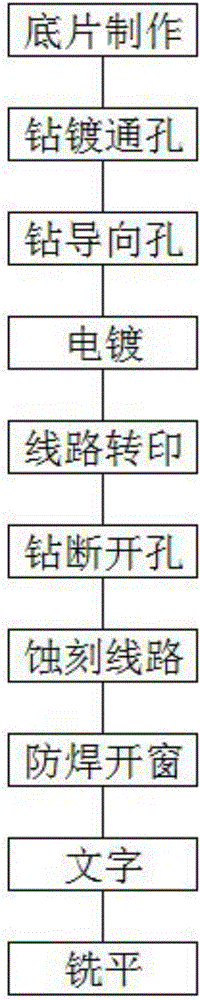
[0038] Such as figure 1 As shown, a PCB pad compensation design process, the steps in turn include:

[0039] ①Negative film production: CAM design of circuit film and solder mask film is carried out according to the original design drawing. The line width of the CAM design circuit is 10% wider than the original design drawing, and the diameter of the CAM design solder mask opening is 20% larger than the original design drawing. At the same time, the solder mask image designed by CAM is designed to compensate the overlapped part of the circuit-solder mask larger than the range of the pad 42, such as Figure 8 ;

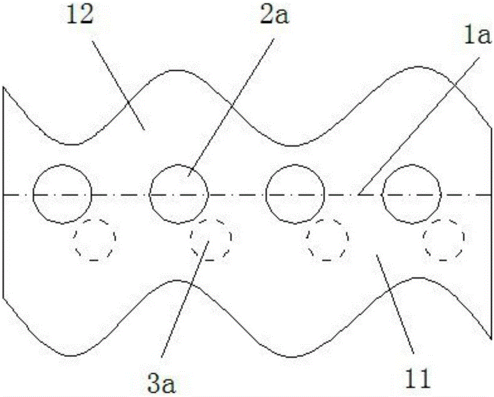
[0040] ②Drilling plated through holes 2a: Drill plated through holes 2a with a diameter of D on the boundary 1a between the removal area 11 and the reserved area 12 of the circuit board;

[0041] ③Drilling guide hole 3a: Drill a guide hole 3a away from the plated through hole 2a in the removal area 12 of the circuit board 1, the diameter of the guide hole 3a is D1 = 0.7D, su...

Embodiment 2

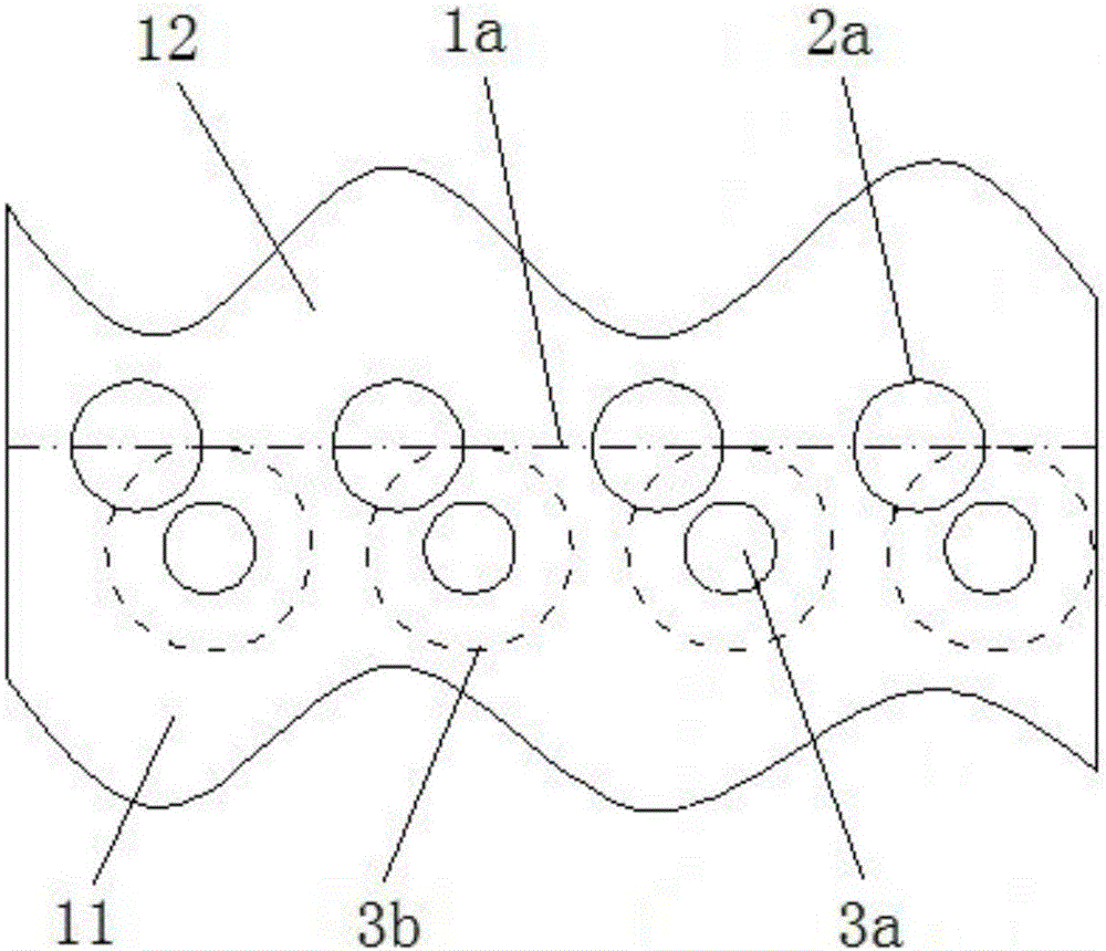
[0053] ①Negative film production: CAM design of the circuit film and solder mask film according to the original design drawing. The line width of the CAM design circuit is 20% wider than the original design drawing, and the diameter of the CAM design solder mask opening is 30% larger than the original design drawing. At the same time, the solder mask image designed by CAM is designed to compensate the overlapped part of the circuit-solder mask larger than the range of the pad 42, such as Image 6 ;

[0054] ②Drilling: Drill a plated through hole 2a with a diameter of D on the boundary 1a between the removal area 11 and the reserved area 12 of the circuit board, and drill a guide that is separated from the plated through hole 2a in the removal area 12 of the circuit board 1 Hole 3a, guide hole 3a diameter D1 = 0.7D, such as figure 2 ;

[0055] ③Plating: Copper film 4 is plated on the surface of the circuit board;

[0056] ④ Circuit transfer: apply exposure ink on the circuit board, ...

Embodiment 3

[0064] Such as Image 6 As shown, the difference from Embodiment 2 is that the drill bit 71 for drilling plated through holes drills through the circuit board 1 and then the drill bit 72 for pilot holes drills through the circuit board 1. Because the plated through hole 2a is a hole that actually needs to be reserved, and the pilot hole 3a is a hole that will be eliminated, the position accuracy of the plated through hole 2a is required to be higher, and it needs to be drilled first. After the plated through-hole drill 71 first drills through the circuit board 1, the circuit board 1 can undergo stress relief and return to flatness, so that the circuit board 1 will not break due to excessive force at the same time when the pilot hole 3a is drilled.


PUM


Abstract

The invention relates to a PCB pad compensation design technology and application thereof, and belongs to the technical field of PCB manufacture. In PCB pad compensation design technology, the line width of a CAM design circuit is greater than that of an original design drawing, the diameter of a solder mask window of CAM design is greater than that of the original design drawing, and a solder mask negative image of CAM design compensates a line-solder mask overlap portion beyond the pad range. Patterns of solder mask windows in a solder mask negative are compensated in design, the shapes of pads formed finally are relatively unified, problems as incomplete soldering and short circuit during tinning can be avoided, and the yield rate of production is improved.

Description

Technical field [0001] The invention relates to the technical field of printed circuit board manufacturing, in particular to a PCB board pad compensation design process and its application for avoiding virtual soldering and short circuit of the pad. Background technique [0002] With the rapid development of the times, the penetration rate of electronic consumer products is getting higher and higher, and the electronic products people are pursuing are also undergoing rapid changes, which also ushered in opportunities and challenges for PCB board manufacturers. Today's electronic products are small, lighter, and thinner. It has brought a test to the process capability of PCB board factories, and solder mask is one of the important processes in printed circuit boards. The solder mask is to expose the part holes and part pads that need to be soldered on the circuit board, and cover the etched circuit and copper surface of the circuit board. When assembling in the downstream proces...

Claims


Application Information

Patent Timeline
IPC IPC(8): H05K3/00
CPCH05K3/0005H05K2203/0528
Inventor 赖荣祥
Owner PLOTECH TECH KUNSHAN CO LTD
Why Eureka
Try Eureka