
A preparation method of low-temperature ohmic contact on gan HEMT

A technology of ohmic contact and low temperature, which is applied in semiconductor/solid-state device manufacturing, semiconductor devices, electrical components, etc., can solve the problems of poor surface morphology of ohmic contact metals, achieve improved flatness and edge quality, large process tolerance, The effect of improving the flatness and edge quality of ohmic metal surfaces

Active Publication Date: 2018-12-28
NO 55 INST CHINA ELECTRONIC SCI & TECHNOLOGYGROUP CO LTD
View PDF6 Cites 0 Cited by
  • Summary
  • Abstract
  • Description
  • Claims
  • Application Information

AI Technical Summary

Problems solved by technology

[0004] The present invention aims at the problem of poor surface morphology of ohmic contact metal caused by high temperature annealing in the ohmic manufacturing process of GaN HEMT devices, and provides a method for reducing the ohmic contact annealing temperature of GaN HEMT devices based on etching and diffusion technology. The method can It can effectively reduce the annealing temperature of GaN HEMT ohmic contact, improve the surface morphology of ohmic contact metal, and can be widely used in the development and production of various GaN HEMT devices

Method used


Image

  • A preparation method of low-temperature ohmic contact on gan HEMT
  • A preparation method of low-temperature ohmic contact on gan HEMT
  • A preparation method of low-temperature ohmic contact on gan HEMT

Examples


Embodiment Construction

[0034] The technical solution of the present invention will be further described below in conjunction with the drawings;

[0035] The invention is a method for reducing the ohmic contact annealing temperature of a GaN HEMT device based on etching and diffusion technology, which includes growing a dielectric layer; making an ohmic contact window; making an ohmic contact through hole; making a diffusion layer; growing a dielectric layer; diffusing; and etching Dielectric layer; making ohmic contact metal. The specific method is as follows"

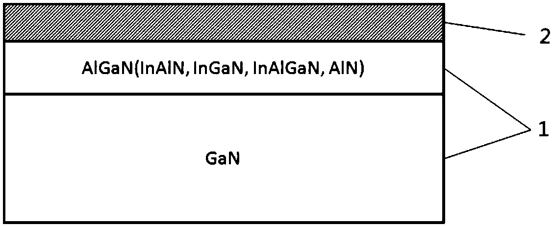
[0036] (1) Using ALD to grow Al with a thickness of 50nm on AlGaN / GaN heterojunction material 1 2 O 3 Medium 2, such as figure 1 Shown. In step (1), the first dielectric layer 2 is prepared by a deposition process, and the first dielectric layer 2 is (Al 2 O 3 ), aluminum nitride (AlN), the deposition method is sputtering, atomic layer deposition, and the dielectric thickness is 50-100nm

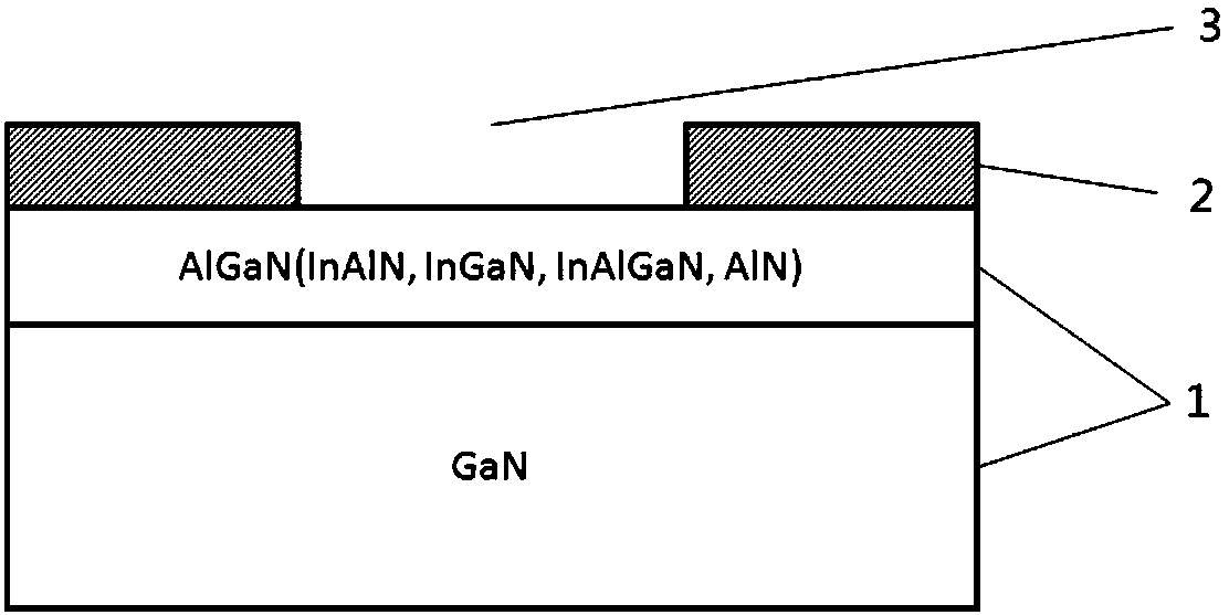
[0037] (2) In Al 2 O 3 The ohmic contact window 3 is prep...


PUM

PropertyMeasurementUnit
thicknessaaaaaaaaaa
thicknessaaaaaaaaaa

Abstract

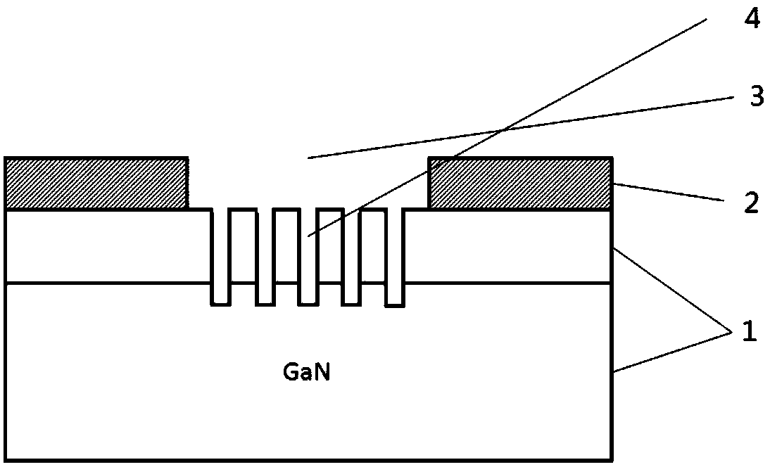
The present invention relates to a method for preparing a low-temperature ohmic contact on a GaN HEMT based on microelectronic technology. The specific implementation steps include: (1) growing a dielectric layer; (2) making an ohmic contact window; (3) making an ohmic contact (4) making a diffusion layer; (5) growing a dielectric layer; (6) diffusing; (7) etching a dielectric layer; (8) making an ohmic contact metal. The present invention aims at the shortcoming of poor morphology of the existing GaN HEMT ohmic contact metal, and proposes to adopt the method of through hole plus diffusion in the ohmic contact area to solve the above problems, which has (1) adopting SiCl4 etching, which increases the concentration of Si in the material; 2) Si diffusion is carried out in the form of through holes, and the process tolerance is large; (3) The temperature of the ohmic alloy is effectively reduced, and the advantages of the surface morphology of the ohmic contact are improved.

Description

Technical field [0001] The invention belongs to the technical field of semiconductor device preparation, in particular to a method for reducing the annealing temperature of ohmic contact by using etching and diffusion technology on a GaN HEMT (gallium nitride high electron mobility transistor). Background technique [0002] The application of GaN as a third-generation semiconductor material in power devices has received extensive attention. Among them, HEMT based on AlGaN / GaN heterojunction structure has the advantages of high frequency, high power density and high operating temperature. It is a solid-state microwave power device and The development direction of power electronic devices. Excellent ohmic contact is the basis for high-performance GaN devices, including low ohmic contact resistivity and good ohmic contact morphology. Ti / Al / Ni / Au is one of the most widely used GaN HEMT ohmic contact metal structures, forming an ohmic contact with GaN through alloys. However, the te...

Claims


Application Information

Patent Timeline
Patent Type & Authority Patents(China)
IPC IPC(8): H01L21/28H01L29/45H01L21/335H01L29/778
CPCH01L21/28H01L29/452H01L29/66462H01L29/778
Inventor 孔岑周建军孔月婵郁鑫鑫郁元卫
Owner NO 55 INST CHINA ELECTRONIC SCI & TECHNOLOGYGROUP CO LTD
Learn More