Preparing method for nanoimprint template
A nano-imprinting and template technology, applied in the field of nano-imprinting, can solve the problems of complicated operation and high cost, and achieve the effects of high repeatability, little structural loss and good shape retention.
- Summary
- Abstract
- Description
- Claims
- Application Information
AI Technical Summary
Problems solved by technology
Method used
Image
Examples
preparation example Construction
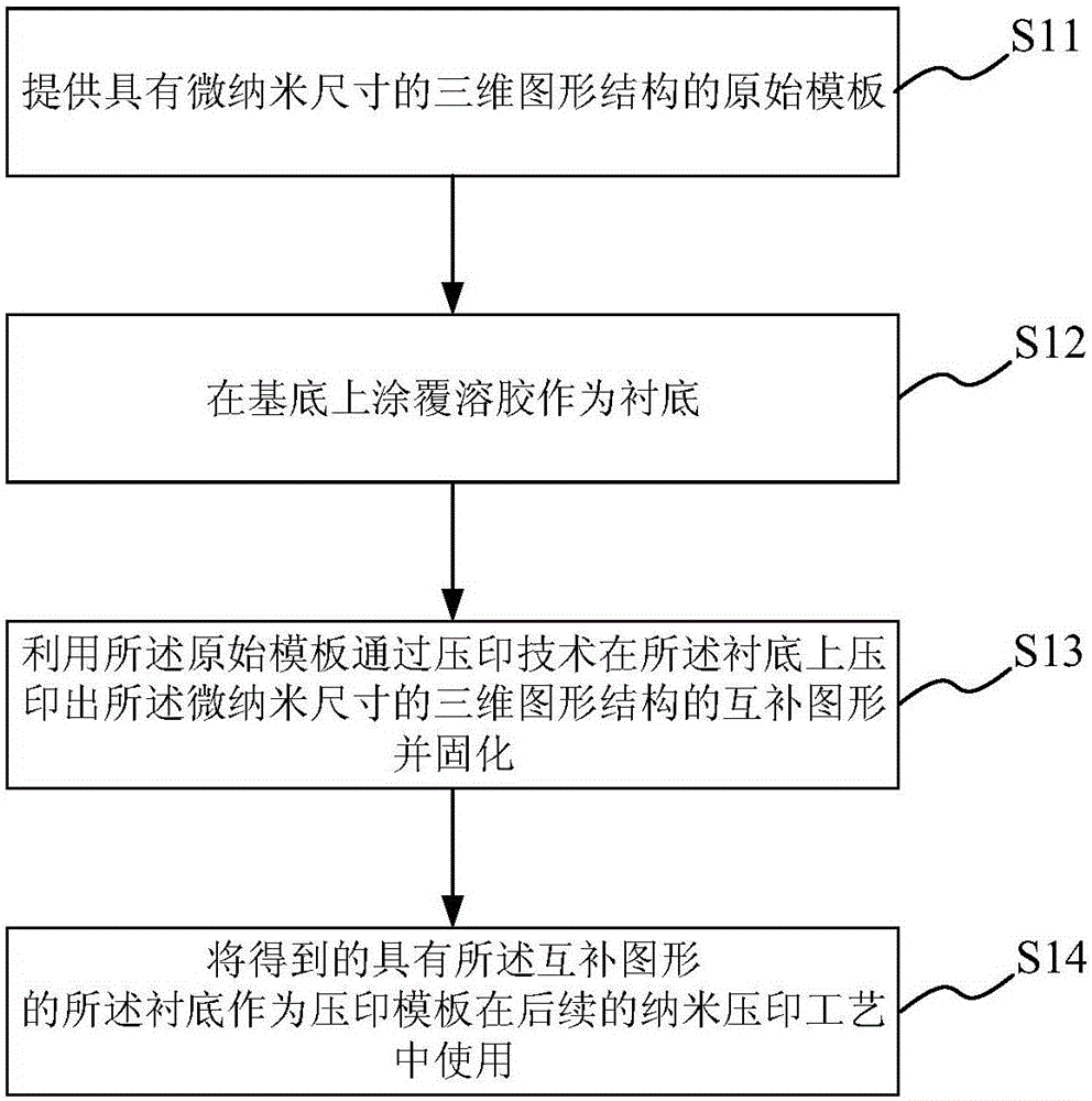
[0052] see figure 1 , the invention provides a method for preparing a nanoimprint template, the method comprising the following steps:
[0053] S11 provides the original template with a three-dimensional graphic structure with micro-nano dimensions;
[0054] S12 coating the sol on the substrate as a substrate;
[0055] S13 using the original template to emboss the complementary pattern of the micro-nano-sized three-dimensional pattern structure on the substrate and solidify;
[0056] S14 using the obtained substrate with the complementary pattern as a template in the subsequent nanoimprint process.
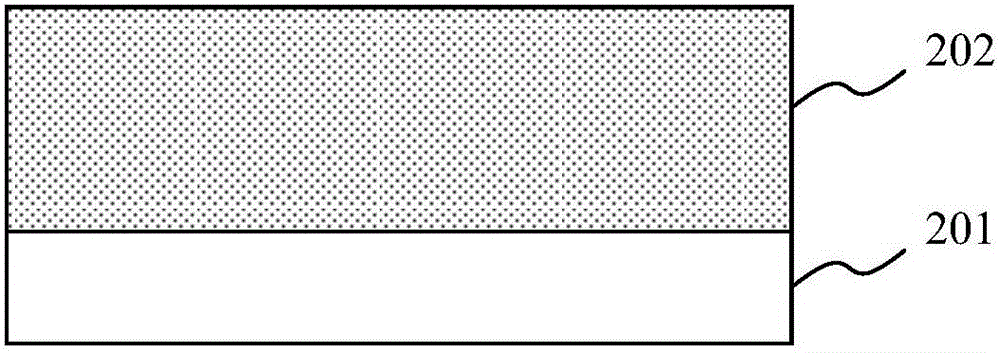
[0057] For specific preparation procedures, please refer to Figure 2a-Figure 2e .
[0058] first as Figure 2a As shown, the original template 101 provided in step S11 has a micro-nano-sized three-dimensional graphic structure, and the micro-nano-sized three-dimensional graphic structure can be columnar, cone-shaped, pyramid-shaped, pit-shaped, inverted cone-shaped, or inver...
Embodiment 1
[0077] In this example, the nanoimprint template preparation method of the present invention is used to prepare TiO 2 Template, and this template is used for flat hot pressing to prepare periodic patterned ETFE film, and its process is as follows:
[0078] 1. Provide a PDMS template with a micro-pit structure as the original template, wherein the micro-pit structure is composed of a plurality of pits of the same shape periodically arranged in an orderly manner, each pit has a depth of 2.45 μm and a diameter of 2.4 μm , the period is 3 μm, that is, the distance between the center of each pit and the center of its adjacent pit is 3 μm. Using a scanning electron microscope (SEM) to observe the surface morphology of the PDMS template, the resulting SEM image is as follows Figure 4 shown.
[0079] 2. Put TiO 2 The sol was spin-coated on a clean glass substrate as a substrate, TiO 2 The thickness of the sol is 5 μm, and the spin coating speed is 1000 revolutions per minute. The...
Embodiment 2
[0088] In this embodiment, the TiO prepared in Example 1 2The template is used for UV imprinting to prepare a periodically patterned photoresist structure, and the preparation process is as follows:
[0089] The ultraviolet imprinting glue is coated on a clean quartz glass substrate, and the thickness of the ultraviolet imprinting glue is 5 μm.
[0090] The TiO prepared in Example 1 2 The template is placed in the UV imprinting chamber, and then the quartz glass substrate coated with UV imprinting glue is placed on the TiO 2 On the template, apply a uniform pressure of 0.25MPa, and irradiate with ultraviolet light, and the irradiation power is 100mW / cm 2 , the irradiation time is 500 seconds.
[0091] After the UV imprinting glue is cured, TiO 2 The template is separated from the UV imprinting glue, that is, a micron-scale pit structure is formed on the quartz glass substrate. The pit depth is 1.370 μm, the diameter is 1.535 μm, and the period is 3 μm. The SEM image of the...
PUM
| Property | Measurement | Unit |
|---|---|---|
| depth | aaaaa | aaaaa |
| diameter | aaaaa | aaaaa |
| thickness | aaaaa | aaaaa |
Abstract
Description
Claims
Application Information


