Beta-Gallium oxide nanowire array film and preparation method thereof
A nanowire array, gallium oxide technology, applied in the field of material science, can solve the problems of difficult to meet practical applications, high dark current of optoelectronic devices, long response time, etc., to achieve the effect of improving optoelectronic performance, short time required, and simple equipment
- Summary
- Abstract
- Description
- Claims
- Application Information
AI Technical Summary
Problems solved by technology
Method used
Image

Examples
preparation example Construction
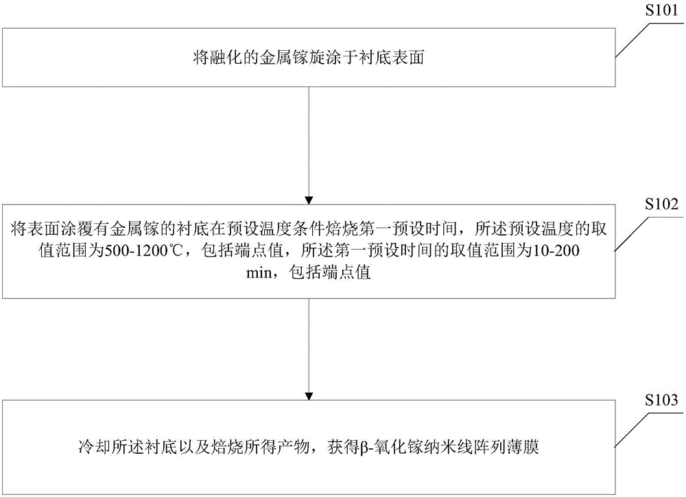
[0035] The embodiment of the present application provides a method for preparing a β-gallium oxide nanowire array film, such as figure 1 shown, including:
[0036] S101: spin-coating molten gallium metal on the surface of the substrate;
[0037] S102: Baking the substrate coated with metal gallium at a preset temperature for a first preset time, the range of the preset temperature is 500-1200°C, including endpoint values, and the first preset time The value range of is 10-200min, including the endpoint value;
[0038] S103: cooling the substrate and firing the obtained product to obtain a β-gallium oxide nanowire array thin film.
[0039] On the basis of the foregoing embodiments, in one embodiment of the present application, said spin-coating molten gallium metal on the surface of the substrate includes:
[0040] S1011: heating and melting the metal gallium with a preset quality;
[0041] S1012: coating molten gallium metal on the surface of the substrate;
[0042] S1013...
Embodiment 1
[0055] In this embodiment, the specific process of the method includes:
[0056] S201: heat and melt 200mg of gallium metal and apply it on the c-plane sapphire substrate;
[0057] S202: placing the c-plane sapphire substrate coated with metal gallium on a spin coater, and rotating at a speed of 5000rpm for 20s;
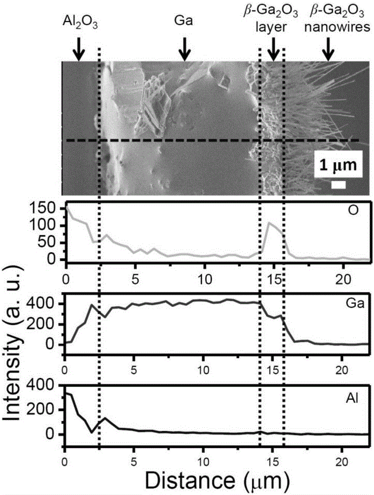
[0058] S203: Baking the spin-coated c-plane sapphire substrate in air or oxygen at a high temperature of 1000° C. for 80 minutes and then cooling to obtain the β-gallium oxide nanowire array film.
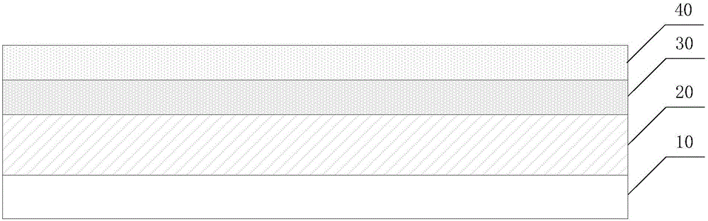
[0059] Next, SEM scanning and XRD testing were performed on the β-gallium oxide nanowire array thin film obtained in Example 1. image 3 It is the SEM photo of the β-gallium oxide nanowire array film obtained in Example 1 and the line scan spectrum of the element distribution at the corresponding position. It can be seen from the figure that the obtained β-gallium oxide nanowire array film has a multilayer structure; From the c-plane sapphire substrate (the main compone...
Embodiment 2
[0063] In this embodiment, in order to examine the influence of the quality of adding metal gallium (ie the preset quality) on the obtained β-gallium oxide nanowire array film, except that the preset quality is different from Example 1, other reactions Conditions were kept the same as in Example 1. That is, the mass of gallium metal in step S201 is set to 10 mg, 100 mg, 300 mg, 500 mg and 1000 mg respectively for experiments.
[0064] The experimental results show that when the preset masses are 10mg, 100mg, 300mg, 500mg and 1000mg respectively, the thicknesses of the metal gallium layer 20 of the prepared β-gallium oxide nanowire array film are 0 μm, 2 μm, 14 μm and 15 μm respectively and 15 μm. The reason may be that when the amount of metal gallium added is too small, a small amount of metal gallium is completely oxidized under high temperature conditions, and before the formation of the β-gallium oxide film 30, the metal gallium has been completely oxidized, resulting in ...
PUM
| Property | Measurement | Unit |
|---|---|---|
| Thickness | aaaaa | aaaaa |
| Length | aaaaa | aaaaa |
| Diameter | aaaaa | aaaaa |
Abstract
Description
Claims
Application Information
 - Generate Ideas
- Intellectual Property
- Life Sciences
- Materials
- Tech Scout
- Unparalleled Data Quality
- Higher Quality Content
- 60% Fewer Hallucinations
Browse by: Latest US Patents, China's latest patents, Technical Efficacy Thesaurus, Application Domain, Technology Topic, Popular Technical Reports.
© 2025 PatSnap. All rights reserved.Legal|Privacy policy|Modern Slavery Act Transparency Statement|Sitemap|About US| Contact US: help@patsnap.com