A flexible fully transparent amorphous oxide thin film transistor and its preparation method
An amorphous oxide, thin film transistor technology, used in transistors, semiconductor/solid-state device manufacturing, semiconductor devices, etc., can solve the problems of low resistivity, poor device stability, reduced on-state current, etc., and achieve good electrical performance. , the effect of high visible light transmittance
- Summary
- Abstract
- Description
- Claims
- Application Information
AI Technical Summary
Problems solved by technology
Method used
Image
Examples
Embodiment 1
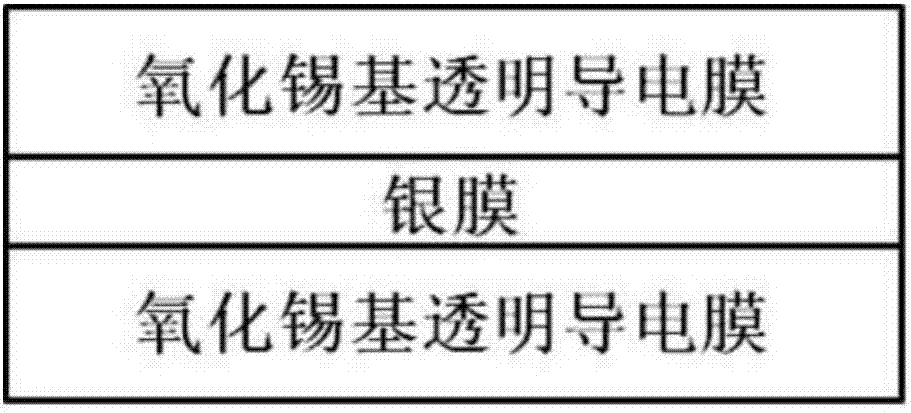
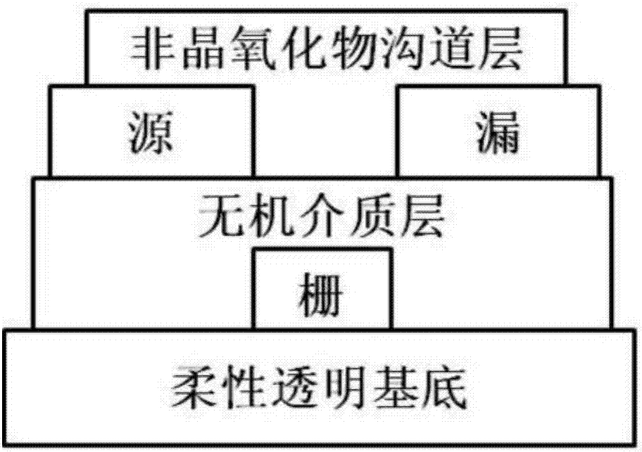
[0037] Using PET as the substrate, amorphous indium gallium zinc oxide (In-Ga-Zn-O) film as the channel layer, inorganic Al 2 o 3 The thin film is used as the dielectric layer, the ITO thin film is used as the gate electrode layer, and the molybdenum (Mo)-doped SnO 2 A silver-based transparent conductive multilayer film composed of transparent conductive oxide and silver film (SnO 2 : Mo / Ag / SnO 2 : Mo) as the source / drain electrode layer, the structure of the silver-based transparent conductive multilayer film is as figure 1 As shown, a flexible fully transparent amorphous oxide TFT with a bottom gate coplanar structure is prepared, and the structure of the flexible fully transparent amorphous oxide TFT is as follows figure 2 As shown, the specific steps are as follows:
[0038] (1) Use radio frequency magnetron sputtering method on the PET substrate to form an ITO film with a thickness of 80nm with the aid of an aluminum oxide mask. The target material is an ITO ceramic ...
Embodiment 2
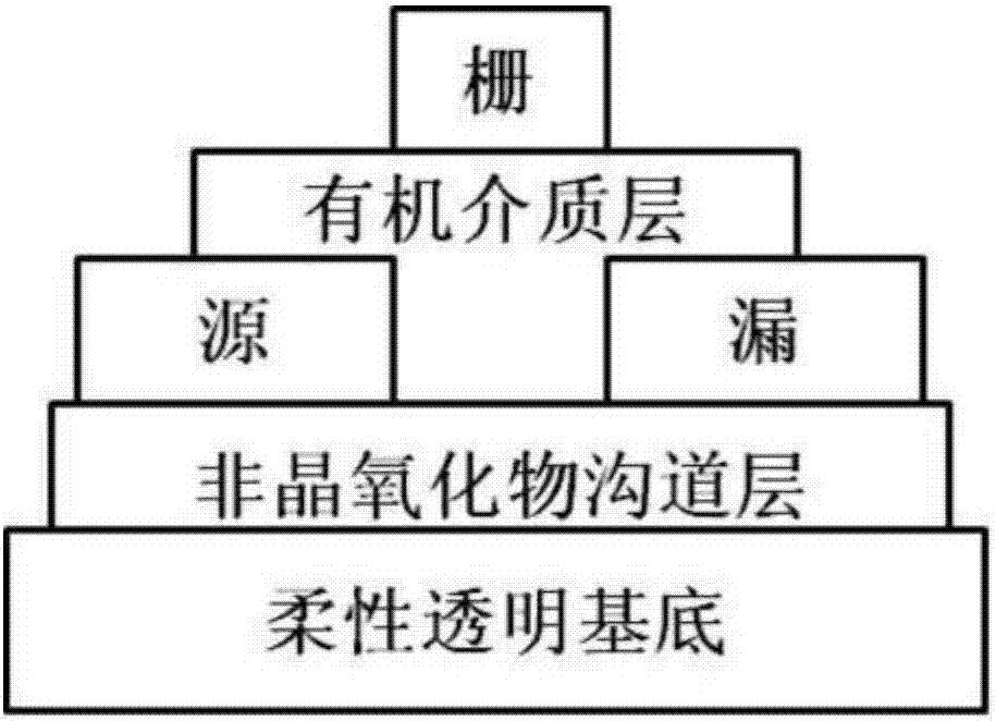
[0044] Using PET as the substrate, amorphous indium gallium zinc oxide (In-Ga-Zn-O) film as the channel layer, organic PMMA film as the dielectric layer, ITO film as the gate electrode layer, molybdenum (Mo) SnO 2 A silver-based transparent conductive multilayer film composed of transparent conductive oxide and silver film (SnO 2 : Mo / Ag / SnO 2 : Mo) as the source / drain electrode layer, the structure of the silver-based transparent conductive multilayer film is as figure 1 As shown, a flexible fully transparent amorphous oxide TFT with a coplanar top gate structure is prepared, and the structure of the flexible fully transparent amorphous oxide TFT is as follows image 3 As shown, the specific steps are as follows:
[0045] (1) An amorphous indium gallium zinc oxide film with a thickness of 50nm is formed on a PET substrate by radio frequency magnetron sputtering. The target material is an indium gallium zinc oxide target with a purity of 4N. The sputtering power is 20W and ...
PUM
| Property | Measurement | Unit |
|---|---|---|
| thickness | aaaaa | aaaaa |
| thickness | aaaaa | aaaaa |
| thickness | aaaaa | aaaaa |
Abstract
Description
Claims
Application Information


