A laser gain chip, laser component, power amplifier and oscillator
A laser gain chip, laser technology, applied in lasers, laser parts, phonon exciters, etc., can solve the problems of difficult to ensure the stability of laser devices, complex structure, bulky and other problems, and achieve the benefits of engineering implementation and convenient operation. , the effect of high gain ability
- Summary
- Abstract
- Description
- Claims
- Application Information
AI Technical Summary
Problems solved by technology
Method used
Image
Examples
Embodiment 1
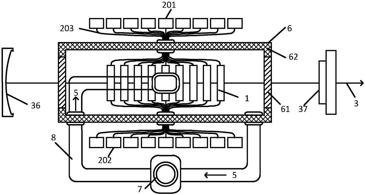
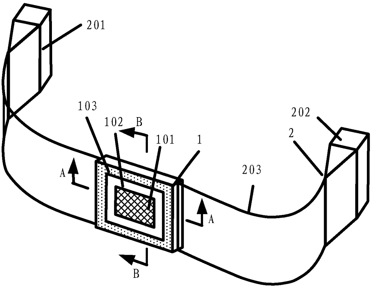
[0044] Such as Figure 1-3 As shown, a laser gain chip includes a laser source, a gain medium 1, a pump source 2 and a cooling fluid 5, the pump source 2 includes a connected diode array and a coupling device 203, and the diode array includes a gain The medium 1 is a diode array one 201 and a diode array one 202 arranged symmetrically to the center, and the diode array one 201 and the diode array one 202 are respectively connected to the gain medium 1 through a coupling device 203, and the coupling device 203 is configured as a strip structure, It is formed by arranging a plurality of optical fibers 204, which are arranged in surface-to-face contact with the gain medium 1, and utilizes the advantage of the flexible transmission of the coupling device 203 to improve the degree of freedom between the diode array and the gain medium 1 in space, so that the pump source 2 and the gain medium 1 are convenient. Arrangement of the gain medium 1 and thermal management.
[0045] The la...
Embodiment 2
[0049] Such as Figure 1-5 As shown, the gain medium 1 is set as a sheet structure, and its interior is set as a graded doping structure along the transmission direction of the pump light 4 to ensure uniform distribution of gain in the gain medium 1. This structure is very suitable for quasi- A three-level gain medium or a gain medium with a low absorption coefficient, the gain medium 1 sequentially includes a central region 101, a transition layer 102 and a cladding layer 103 from the inside to the outside, and the central region 101 and the cladding layer 103 are all set to be gradually doped structure, the active ions doped inside the central region 101 are Nd 3+ or Yb 3+ , thereby ensuring that the pump light 4 is absorbed in the central region 101, and the corresponding doped active ions inside the cladding layer 103 are Sm 3+ or Cr 4+ , which absorb less pumping light 4, have high absorption efficiency for spontaneous emission of laser light 3, suppress the lateral se...
Embodiment 3
[0052] Such as figure 1 , 6 As shown, a laser component includes the above-mentioned laser gain chip, and multiple laser gain chips are cascaded along the laser transmission direction to realize power expansion. Each gain medium 1 has an independent pump source 2, and each gain medium 1 has an independent pump source 2, and each The same small-signal gain can be obtained in the gain medium 1, and the gain distribution is uniform, and the absorbed pump energy and heat generation density have the same distribution. In the process of power expansion, there is no need to consider the influence of other factors, and the operation is convenient. At the same time, The distance between adjacent laser gain chips is on the order of millimeters, preferably 0.5-5mm, with a compact structure and a small occupied space.
[0053] The laser assembly is arranged inside the laser assembly housing 6, the laser assembly housing 6 includes a window 61 and a housing 62, the window 61 is coated wit...
PUM
 Abstract
Description
Claims
Application Information


