Spintronics device based on metamaterial
A technology of spintronics and metamaterials, applied in electrical components, semiconductor devices, circuits, etc., can solve problems such as high frequency of spintronics devices, integration and wireless obstacles
- Summary
- Abstract
- Description
- Claims
- Application Information
AI Technical Summary
Problems solved by technology
Method used
Image
Examples
Embodiment Construction
[0035]The present invention will be further described below in conjunction with the accompanying drawings and embodiments, which are not intended to limit the claims of the present invention.
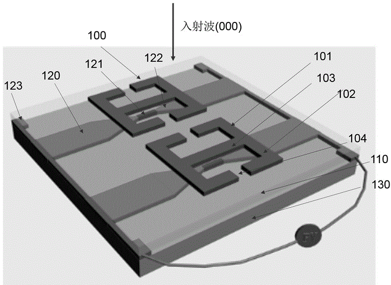
[0036] figure 1 It is the metamaterial-based spin rectification device of the present invention, specifically a three-layer structure: the upper layer structure 100 is composed of periodically arranged back-to-back split resonant rings SRRs101 and 102, and the middle strip 103 of the SRRs will generate an extremely strong current during resonance , which provides a very strong magnetic field for the metal ferromagnetic material; the middle is composed of a medium 110, which is mainly used as the isolation between the substrate of the upper structure and the upper and lower layers, and the microcavity of the resonator; the lower layer is Metal strips 120 and metal magnetic materials 121 are compounded. The width of the metal strips gradually narrows 122. It is the narrowest right below ...
PUM
| Property | Measurement | Unit |
|---|---|---|
| Thickness | aaaaa | aaaaa |
Abstract
Description
Claims
Application Information


