A kind of bipolar resistive variable memory and preparation method thereof

A resistive variable memory and bipolar technology, applied in the direction of electrical components, etc., can solve problems such as the inability to use RRAM, the difficulty of high-density three-dimensional integration, and the inability to take advantage of the scalability of RRAM.

Active Publication Date: 2019-03-15
合肥中科微电子创新中心有限公司
View PDF8 Cites 0 Cited by
  • Summary
  • Abstract
  • Description
  • Claims
  • Application Information

AI Technical Summary

Problems solved by technology

The 1T1R structure can effectively solve the problem of crosstalk, but the area of ​​the memory unit mainly depends on the area of ​​the transistor, which cannot take advantage of the excellent scalability of RRAM, and it is difficult to carry out high-density three-dimensional integration; area, and is also conducive to high-density three-dimensional integration, but diodes usually only have unidirectional conduction characteristics, so they can only be used for unipolar RRAMs, not bipolar RRAMs

Method used


Image

  • A kind of bipolar resistive variable memory and preparation method thereof
  • A kind of bipolar resistive variable memory and preparation method thereof
  • A kind of bipolar resistive variable memory and preparation method thereof

Examples


preparation example Construction

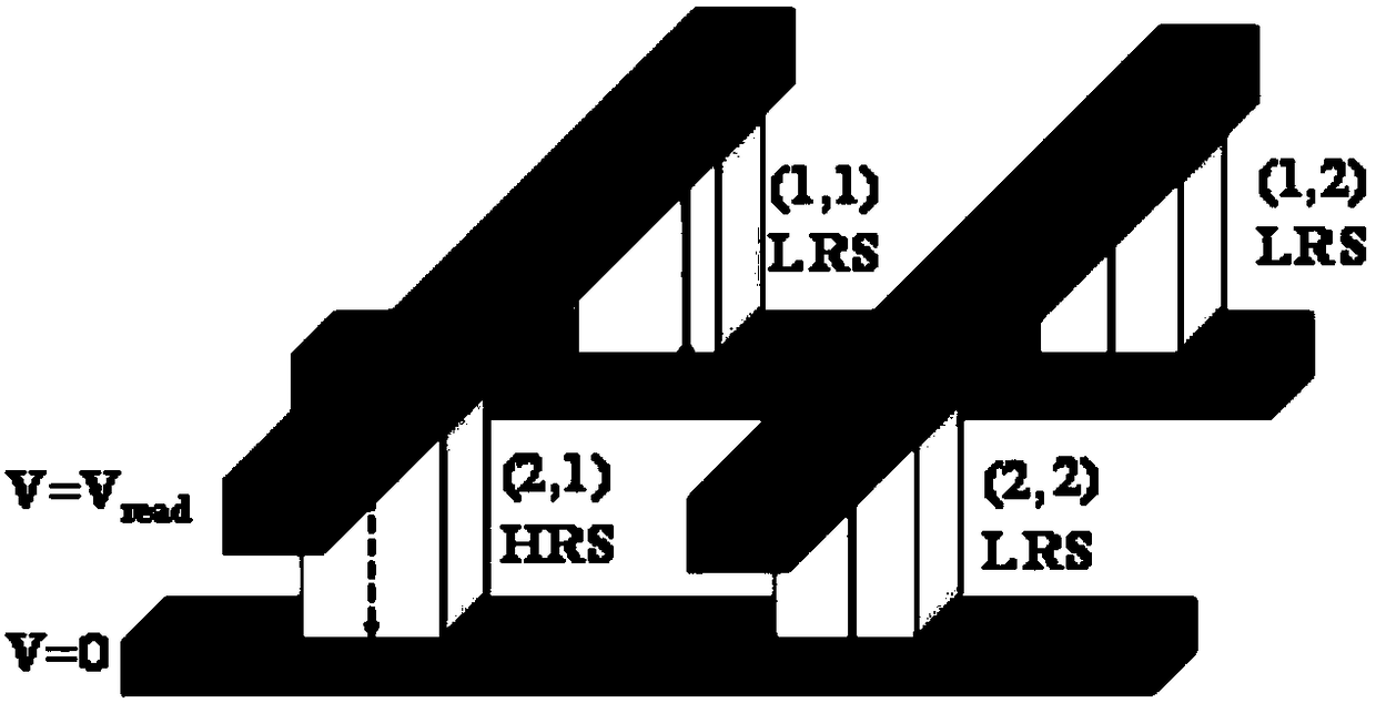
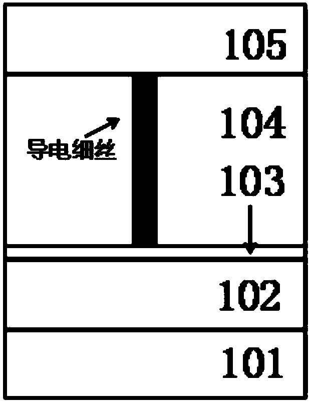
[0057] The present invention also provides a method for preparing the bipolar resistive memory, comprising: S1) providing a substrate; S2) forming a lower electrode on the upper surface of the substrate; S3) depositing rectification functional layer; the rectification functional layer is made of Al 2 o 3 、TiO 2 Forming with one or more of MgO; S4) transferring the graphene film to the rectification function layer to form a graphene layer; S5) depositing a resistive medium layer on the graphene layer; S6) forming a graphene layer on the graphene layer; An upper electrode is deposited on the resistive medium layer to obtain a bipolar resistive memory.

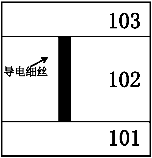
[0058] Wherein, the substrate, the lower electrode, the rectifying functional layer, the graphene layer, the resistive medium layer and the upper electrode are all the same as above, and will not be repeated here; see Figure 4 , Figure 4 It is a schematic diagram of the preparation process of the bipolar resistive memory of...

Embodiment 1

[0068] 1.1 Provide substrate SiO 2 / Si.

[0069] 1.2 Deposit metal Pt50nm and Ti10nm on the substrate as the bottom electrode by E-beam evaporation process.

[0070] 1.3 Deposit 3nm Al on the bottom electrode by magnetron sputtering 2 o 3 A rectification functional layer is formed.

[0071] 1.4 Transfer the single-layer graphene obtained by the chemical vapor deposition (CVD) process on the copper sheet to the rectifying functional layer to form a graphene layer by a peeling transfer process.

[0072] 1.5 Deposit 10nm HfO on the graphene layer by magnetron sputtering 2 As a resistive dielectric layer.

[0073] 1.6 Deposit 70nm metal Cu as the upper electrode on the resistive dielectric layer by electron beam evaporation process.

[0074] 1.7 Deposit 10nm metal Au as a protective layer on the upper electrode by electron beam evaporation process.

Embodiment 2

[0076] 2.1 Provide substrate SiO 2 / Si.

[0077] 2.2 Deposit metal Au50nm and Ti10nm on the substrate as the bottom electrode by E-beam evaporation process.

[0078] 2.3 Deposit 3nm MgO on the lower electrode by magnetron sputtering to form a rectifying functional layer.

[0079] 2.4 Transfer the bilayer graphene obtained by the chemical vapor deposition (CVD) process on the copper sheet to the rectifying functional layer to form a graphene layer by a peeling transfer process.

[0080] 2.5 Deposit 10nm ZrO on the graphene layer by magnetron sputtering 2 As a resistive dielectric layer.

[0081] 2.6 Deposit 70nm metal Ag on the resistive medium layer by electron beam evaporation process as the upper electrode.

[0082] 2.7 Deposit 10nm metal Au as a protective layer on the upper electrode by electron beam evaporation process.


PUM


Abstract

The invention provides a bipolar resistive memory and a preparation method thereof. The bipolar resistive memory comprises a substrate; a lower electrode compounded on the upper surface of the substrate; a rectification function compounded on the lower electrode layer; a graphene layer compounded on the rectifying functional layer; a resistive dielectric layer compounded on the graphene layer; an upper electrode compounded on the resistive dielectric layer; the rectifying functional layer is composed of Al 2 o 3 、TiO 2 Formed with one or more of MgO. Compared with the prior art, the rectification functional layer in the bipolar resistive memory provided by the present invention can play the role of tunnel rectification, realize bidirectional rectification, and can also effectively suppress the gap between adjacent cells in the resistive memory array. The phenomenon of crosstalk misreading; at the same time, due to the existence of the graphene layer, the performance of the device is improved, the reset current is reduced, the response speed is improved, and the power consumption is reduced.

Description

technical field [0001] The invention belongs to the technical field of micro-nano electronic devices and memories, and in particular relates to a bipolar resistive memory and a preparation method thereof. Background technique [0002] With the continuous improvement of people's requirements for electronic equipment and the popularity of portable electronic equipment, the share of non-volatile memory in the entire memory market continues to expand. At present, FLASH storage technology is still the mainstream of the non-volatile memory market, accounting for more than 90% of the market share. However, with the continuous innovation of microelectronics and semiconductor technology, FLASH storage technology is facing a series of bottleneck problems, such as the impossibility of unlimited thinning of the floating gate with the development of technology, limited data retention time, excessive operating voltage, and high operating speed. Wait for a series of questions. The existe...

Claims


Application Information

Patent Timeline
Patent Type & Authority Patents(China)
IPC IPC(8): H01L45/00
CPCH10N70/8418H10N70/021
Inventor 刘琦赵晓龙刘明刘森龙世兵吕杭炳卢年端王艳张康玮
Owner 合肥中科微电子创新中心有限公司
Why Eureka
Try Eureka