Packaging structure and packaging method for silicon carbide power device

A technology of power devices and packaging structures, which is applied in the manufacture of semiconductor devices, electrical solid state devices, and semiconductor/solid state devices. Coupling, the effect of reducing contact resistance and parasitic inductance

Active Publication Date: 2016-08-31
HUAZHONG UNIV OF SCI & TECH
View PDF5 Cites 16 Cited by
  • Summary
  • Abstract
  • Description
  • Claims
  • Application Information

AI Technical Summary

Problems solved by technology

Among them, the bonding wire has a simple structure and high reliability, but the package size on one side is large and the parasitic inductance is large; the flat plate structure has small parasitic parameters and good heat dissipation, but the process is complicated and the reliability is poor; the hybrid packaging structure is a bonded wire structure and The combination of direct copper-clad ceramic substrate technology has the advantages of both, but the existing hybrid packaging structure still has the problems of large parasitic parameters, small soldering area resulting in reduced reliability, and the need for external terminals to connect to external circuits. Therefore, it is necessary Optimize the packaging structure and packaging method

Method used


Image

  • Packaging structure and packaging method for silicon carbide power device
  • Packaging structure and packaging method for silicon carbide power device
  • Packaging structure and packaging method for silicon carbide power device

Examples


Embodiment Construction

[0052] In order to make the object, technical solution and advantages of the present invention clearer, the present invention will be further described in detail below in conjunction with the accompanying drawings and embodiments. It should be understood that the specific embodiments described here are only used to explain the present invention, not to limit the present invention. In addition, the technical features involved in the various embodiments of the present invention described below can be combined with each other as long as they do not constitute a conflict with each other.

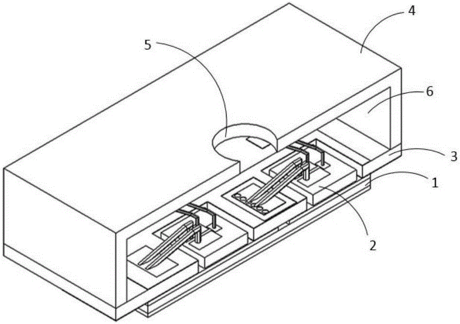
[0053] Such as figure 1 As shown, it is a schematic cross-sectional view of a package structure of a silicon carbide power device provided by an embodiment of the present invention. The package structure includes a DBC substrate 1 , a silicon carbide power device, a PCB board 3 , and a housing 4 .

[0054] The PCB board 3 and the silicon carbide power device are welded on the DBC substrate 1; t...


PUM

PropertyMeasurementUnit
diameteraaaaaaaaaa

Abstract

The invention discloses a packaging structure and a packaging method for a silicon carbide power device. The packaging structure comprises a direct bond copper (DBC) ceramic substrate, a silicon carbide power device, a PCB, leads and a shell and forms a half-bridge circuit structure formed by the silicon carbide power device. According to the packaging structure and the packaging method provided by the invention, the area of a power circuit can be effectively reduced, conductors with opposite current flowing directions are formed during a commutation process by a switch transistor, mutual inductance offset is used for reducing parasitic inductance of a commutation circuit, and overvoltage and oscillation during the switching process can be effectively reduced; driving signal leads adopt a Kelvin connection mode and are vertical to power leads, a role of effectively reducing coupling between a driving circuit and a power circuit is played, and driving stability is enhanced; the DBC substrate and the PCB are welded thoroughly, and packaging reliability is enhanced; and power terminals and signal terminals are directly included in the PCB, thereby reducing contact resistance and parasitic inductance brought by extra terminals and achieving effects of reducing the cost.

Description

technical field [0001] The invention belongs to the technical field of integrated circuits, and more specifically relates to a packaging structure and a packaging method of a silicon carbide power device. Background technique [0002] As a wide-bandgap semiconductor material, silicon carbide semiconductor not only has high breakdown electric field strength and good thermal stability, but also has the characteristics of high carrier saturation drift speed and high thermal conductivity. It can be used to manufacture various high temperature resistant high High-frequency, high-efficiency and high-power devices are used in occasions where traditional silicon devices are incompetent. In theory, the switching frequency of silicon carbide devices can reach up to megahertz, but the packaging structure of existing commercial devices greatly limits the high-frequency application of silicon carbide devices, mainly due to the noise caused by the interconnection of substrates, chips, and...

Claims


Application Information

Patent Timeline
Patent Type & Authority Applications(China)
IPC IPC(8): H01L23/02H01L23/488H01L25/00H01L21/50H01L21/52H01L21/60
CPCH01L24/06H01L24/80H01L25/00H01L21/50H01L21/52H01L23/02H01L23/488H01L2224/061H01L2224/4903
Inventor 陈材黄志召李宇雄方建明陈宇康勇
Owner HUAZHONG UNIV OF SCI & TECH
Why Eureka
Try Eureka