A soi LDMOS device with buried oxygen field plate

A field plate and device technology, applied in the field of SOILDMOS devices, can solve problems such as limiting the application of SOI devices, and achieve the effect of improving the self-heating effect

Active Publication Date: 2019-04-02
HANGZHOU DIANZI UNIV
View PDF5 Cites 0 Cited by
  • Summary
  • Abstract
  • Description
  • Claims
  • Application Information

AI Technical Summary

Problems solved by technology

The self-heating effect will bring a series of adverse effects on the device, such as: the negative differential mobility of the carriers and the decrease of the saturated output current, which seriously limits the application of SOI devices in the field of high temperature and high power

Method used


Image

  • A soi LDMOS device with buried oxygen field plate
  • A soi LDMOS device with buried oxygen field plate
  • A soi LDMOS device with buried oxygen field plate

Examples


Embodiment Construction

[0019] In order to make the objectives, technical solutions and advantages of the present invention clearer, the present invention will be described in detail below with reference to the accompanying drawings.

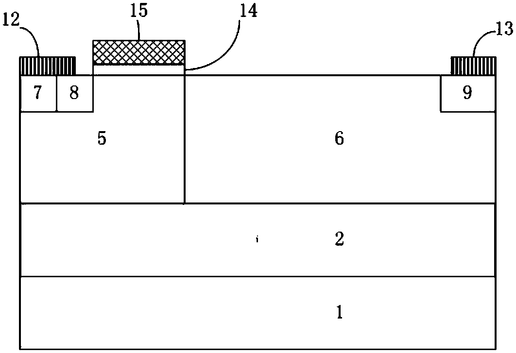
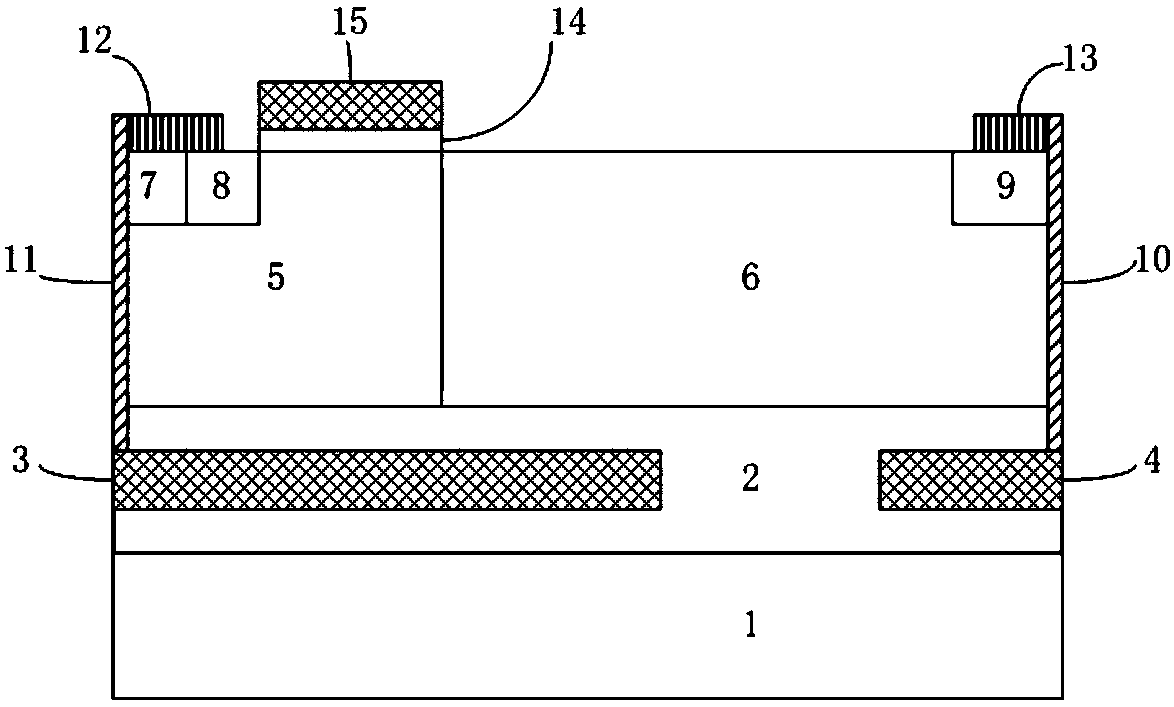
[0020] Such as figure 1 As shown, it is an existing SOI LDMOS device, such as figure 2 As shown, an SOI LDMOS device with a buried oxygen field plate includes a P-type substrate 1, a buried oxide layer 2, a channel region 5, a drift region 6, a source P+ region 7, a source N+ region 8, and a drain N+ region 9, source 12, drain 13, gate 15 and gate oxide layer 14. It is characterized in that it also includes source buried oxygen field plate 3, drain buried oxygen field plate 4, first connection metal 10, and second connection Metal 11; the buried oxygen layer 2 is provided with a source buried oxygen field plate 3 and a drain buried oxygen field plate 4; the drain 13 is connected to the drain buried oxygen field plate 4 through a first connecting metal 10, and the source ...


PUM


Abstract

The invention discloses an SOI LDMOS (Silicon On Insulator Laterally Double-Diffused MOSFET) device with buried field plates, and relates to a semiconductor power device. The SOI LDMOS device comprises a P-type substrate, buried oxide layers, the buried field plates, top silicon, transverse polysilicon gate, a source electrode, a drain electrode, a metal electrode and a gate oxide layer. The SOI LDMOS device is provided with the source and drain buried oxide plates; due to the introduction of the drain buried oxide plate, a drift region in an N<+> drain region is shielded, so that a longitudinal voltage of the device is applied to the buried oxide layer in the drain buried field plate; due to the introduction of the source buried field plate, body exhaustion of the device is enhanced and transverse electric field distribution of the device is modulated, so that a breakdown voltage of the device is increased and on-resistance is reduced; and in addition, the buried field plates replace part of buried oxide layers and the heat conductivity of polysilicon is greater than that of silicon dioxide, so that a self-heating effect of the device can be effectively improved.

Description

Technical field [0001] The invention relates to a semiconductor power device, in particular to an SOI LDMOS device with a buried oxygen field plate. Background technique [0002] SOI (Silicon On Insulator) technology has the advantages of low leakage, low parasitic capacitance, low power consumption, high reliability, and easy isolation. It is widely used in various smart power integrated circuits (Smart Power Integrated Circuit, SPIC) and high voltage integration. Circuit (High Voltage Integrated Circuit, HVIC), and is called "21st Century Silicon Integrated Technology". [0003] SOI LDMOS (Laterally Double-Diffused MOSFET) devices have been widely used in automotive electronics, aerospace and other fields due to their excellent electrical performance. In addition, SOI LDMOS devices, as the core high-voltage power devices in SPIC and HVIC, usually need to work in a high-voltage, high-current state. But the specific on-resistance of LDMOS devices (SpecificOn-resistance, R on,sp T...

Claims


Application Information

Patent Timeline
Patent Type & Authority Patents(China)
IPC IPC(8): H01L29/78H01L29/40
CPCH01L29/407H01L29/7824
Inventor 王颖王祎帆于成浩曹菲
Owner HANGZHOU DIANZI UNIV
Why Eureka
Try Eureka