Optical fingerprint recognition device forming method

A fingerprint identification and optical technology, applied in the field of image processing, can solve the problems of long optical path, high cost, poor accuracy, etc., and achieve the effect of reducing costs

Active Publication Date: 2016-09-21
GALAXYCORE SHANGHAI
View PDF5 Cites 6 Cited by
  • Summary
  • Abstract
  • Description
  • Claims
  • Application Information

AI Technical Summary

Problems solved by technology

[0004] However, the current optical fingerprint identification devices are large in size and have a long optical path, so they cannot be applied to portable electronic devices such as mobile phones
Under the premise of limited volume, the fingerprint recognition device suitable for portable electronic devices such as mobile phones needs to use a lens with a finer and more complex three-dimensional surface to ensure the required optical properties, such as resolution. However, using traditional micro-processing technology, For example, anisotropic or isotropic dry etching and wet etching can only process surfaces with limited topography, and newly developed three-dimensional micromachining technologies such as multi-layer mask technology, laser three-dimensional lithography, and electron beam direct writing technology , there are problems such as poor accuracy, high cost, and low output, which cannot meet the production requirements of such high-precision devices.

Method used


Image

  • Optical fingerprint recognition device forming method
  • Optical fingerprint recognition device forming method
  • Optical fingerprint recognition device forming method

Examples


Embodiment Construction

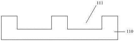
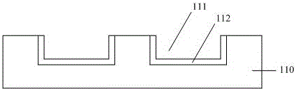
[0020] In order to solve the above-mentioned problems in the prior art, the present invention provides a method for forming an optical fingerprint identification device. The lens array is formed by the gradual light flux lithography method, which can meet the requirements for more precise and complex lens production, and accurately ensure the accuracy of optical fingerprints. The optical characteristics required for identification devices are suitable for portable electronic devices and are compatible with existing chip fabrication and packaging processes to reduce costs.

[0021] In the following detailed description of the preferred embodiment, reference is made to the accompanying drawings which form a part hereof. The accompanying drawings show, by way of example, specific embodiments in which the invention can be practiced. The illustrated embodiments are not intended to be exhaustive of all embodiments in accordance with the invention. It is to be understood that other ...


PUM


Abstract

The invention provides an optical fingerprint recognition device forming method, and the method comprises the steps: a silicon substrate is provided, a groove array is formed on the silicon substrate; a light transmission substrate and an image sensor chip are provided and bonded, a lens array is formed on the light transmission substrate through a gray-tone lithography method, and the lens array is corresponding to a photosensitive array of the image sensor chip; the groove surface of the silicon substrate is bonded with the light transmission substrate, the groove array is corresponding to the lens array, un-grooved surface of the silicon substrate is etched to expose the lens array, and a silicon diaphragm is formed between adjacent lens. According to the invention, the lens array can be formed through the gray-tone lithography method, the precise and complex lens production request can be met, the optical properties needed by an optical fingerprint recognition device can be accurately ensured, the method is suitable for portable electronic equipment and is compatible with the chip production and packaging technology in prior art, so that the cost can be reduced.

Description

technical field [0001] The invention relates to the field of image processing, in particular to a method for forming an optical fingerprint identification device. Background technique [0002] The current fingerprint identification schemes include optical technology, silicon technology (capacitive / radio frequency type), ultrasonic technology, etc. [0003] Optical technology The use of optical imaging equipment is based on the principle of total reflection of light (FTIR). The light hits the surface of the glass with fingerprints, and the reflected light is obtained by the image sensor. The amount of reflected light depends on the depth of the fingerprint ridges and valleys pressed on the surface of the glass, as well as the oil and moisture between the skin and the glass. After the light is shot to the center of the valley through the glass, it is totally reflected at the interface between the glass and the air, and the light is reflected to the image sensor, while the lig...

Claims


Application Information

Patent Timeline
Patent Type & Authority Applications(China)
IPC IPC(8): G06K9/00
CPCG06V40/1324
Inventor 赵立新陈俭夏欢
Owner GALAXYCORE SHANGHAI
Why Eureka
Try Eureka